Expanding Investment Amid Growing AI Demand
Factory Completion Targeted for 2026
Strengthening Expertise and Technology Partnerships
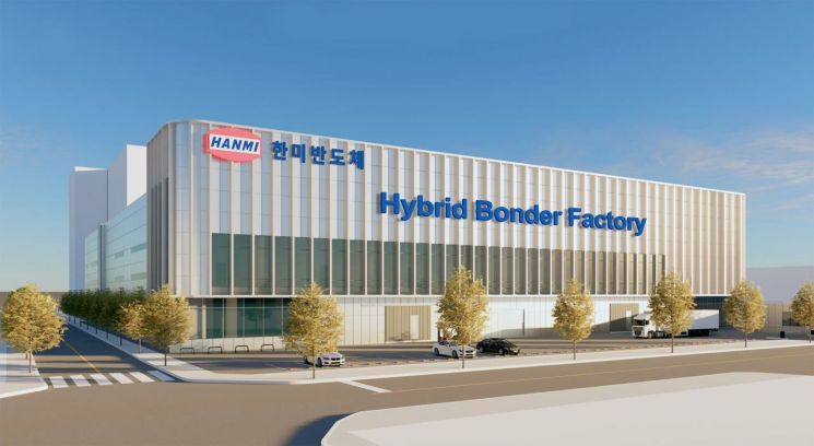
Hanmi Semiconductor has announced an investment of 100 billion KRW in hybrid bonding technology. The company plans to launch hybrid bonder equipment by the end of 2027.
According to Hanmi Semiconductor on July 25, the company is investing a total of 100 billion KRW to build a hybrid bonder factory in the Juan National Industrial Complex in Seo-gu, Incheon. The facility will have a total floor area of 4,415 pyeong (14,570.84 square meters) and will be two stories above ground. Completion is targeted for the second half of 2026. With this investment, Hanmi Semiconductor will complete a production line with a total area of 27,083 pyeong (89,530 square meters).
At the hybrid bonder factory, Hanmi Semiconductor plans to produce next-generation equipment, including high-spec TC bonders for HBM, fluxless bonders, big die TC bonders for AI 2.5D packages, and hybrid bonders (for HBM and logic semiconductor XPU). TC bonders are core semiconductor packaging equipment that precisely attach chips to substrates. They are especially essential for producing high-performance memory such as HBM. HBM is a key component that determines the computing performance of AI (artificial intelligence) semiconductors, and demand is rapidly increasing. According to industry sources, Samsung Electronics is expected to apply hybrid bonders to sixth-generation HBM (HBM4), while SK hynix is expected to use them for seventh-generation products (HBM4E).
Hanmi Semiconductor is also strengthening its technology development. On July 23, Hanmi Semiconductor signed a hybrid bonder technology agreement with semiconductor equipment company TES. The company expects that combining Hanmi Semiconductor's bonder technology for HBM with TES's plasma, thin film deposition, and cleaning technologies will enhance competitiveness. Additionally, Hanmi Semiconductor plans to accelerate technology development by reinforcing its hybrid bonder research and development (R&D) personnel.
Hanmi Semiconductor also plans to supply HBM TC bonder equipment, which holds the number one market share, according to its roadmap. Production of the HBM4-dedicated equipment 'TC Bonder 4,' which was launched in May, began this month, and the launch of fluxless bonder equipment is also scheduled within this year.
A Hanmi Semiconductor representative stated, "Hybrid bonding technology is required to improve the performance of next-generation high-stacking HBM. Through proactive investment, Hanmi Semiconductor will continue its market leadership by supplying the core equipment needed for global memory companies' next-generation HBM development in a timely manner."
Founded in 1980, Hanmi Semiconductor is a semiconductor equipment company with more than 320 customers worldwide. Since establishing its Intellectual Property Division in 2002, the company has filed approximately 120 patents in the field of HBM-related equipment alone.
© The Asia Business Daily(www.asiae.co.kr). All rights reserved.


