Advanced Technology and Production Speed Ahead of Global Competitors
Technical Challenges Emerge Amid Growing Adoption of Glass Substrates
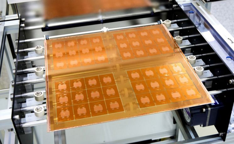
SKC subsidiary Absolics has been producing glass substrate samples and delivering them to clients since the second half of last year. This marks the first move to secure market share amid a wave of major companies entering the glass substrate business.
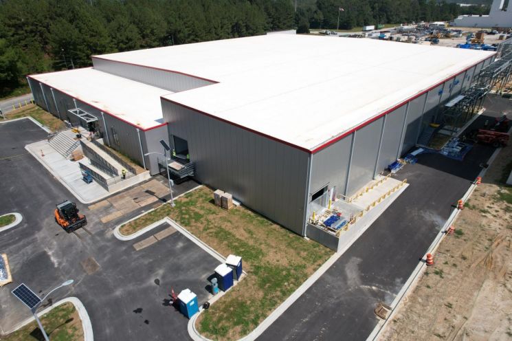 A view of the Absolix glass substrate mass production factory located in Covington, Georgia, USA. Provided by Absolix
According to industry sources on the 15th, Absolics is manufacturing glass substrates and supplying samples to key clients. These clients use the samples to apply to their products or processes, testing performance, quality, and compatibility. An SKC official stated, "We are currently in discussions with several big tech companies aiming for mass production by the end of this year."
It is understood that Absolics has provided samples to up to 20 companies. While SKC has expressed difficulty in disclosing client information, Chris Tip, Absolics' Marketing Director, mentioned in an interview with SKC's PR channel last year that "right after the glass substrate factory began operations, more than 20 influential global semiconductor companies showed interest and contacted us first."
Absolics' early delivery of glass substrate samples is notable compared to other companies. Competitors Samsung Electro-Mechanics and LG Innotek have only just entered the market. Overseas, Japanese materials company Dainippon Printing (DNP) aims for mass production of glass substrates by 2027. Ibiden, the world's top semiconductor substrate manufacturer, exclusively supplies AI semiconductor substrates to Nvidia but only included glass substrates as a research and development project starting in 2023, currently at the initial stage.
Last year, Absolics completed the world's first mass production plant for glass substrates in Georgia, USA. An industry insider said, "Absolics leads the industry in prototype production and mass production preparation speed," adding, "They possess advanced technology ahead of competitors in manufacturing large-area substrates, a critical requirement for artificial intelligence (AI) semiconductors."
Absolics continues to increase hiring ahead of full-scale mass production. They are currently recruiting for positions including process integration engineers, process and product development engineers, electrical modeling and simulation engineers, research program managers, and production supervisors. Over 500 applicants have already applied through the business social media platform LinkedIn for this recruitment.
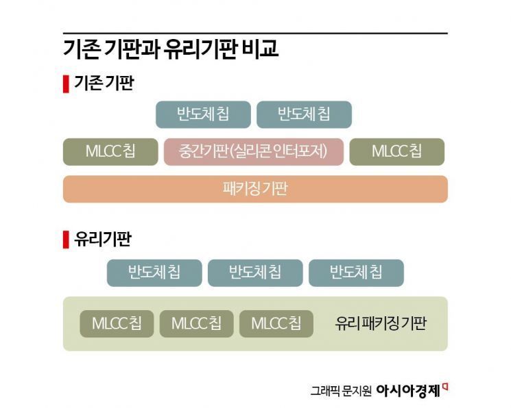
Glass substrates can be used without intermediate parts (interposers) placed between the chip and substrate, allowing for thinner substrates. Power consumption is reduced by 30%, processing speed increases by 40%, and production time is cut in half. Director Tip stated, "Using glass substrates allows circuit line widths to be reduced to about 2 μm (micrometers, one-millionth of a meter) and also reduces costs."
Semiconductor companies expected to become glass substrate clients are also pushing for adoption. Intel has officially announced plans to adopt glass substrates before 2030, and AMD and Broadcom are reviewing the technology. Nvidia is also rumored to be considering glass substrate adoption.
However, technical challenges remain high, with many issues to resolve in the manufacturing process. Do-yeon Choi, a researcher at SK Securities, said, "Time is needed to verify durability in through-glass vias (TGV), yield during mass production, and reliability due to new supply chain arrangements."
© The Asia Business Daily(www.asiae.co.kr). All rights reserved.
![Clutching a Stolen Dior Bag, Saying "I Hate Being Poor but Real"... The Grotesque Con of a "Human Knockoff" [Slate]](https://cwcontent.asiae.co.kr/asiaresize/183/2026021902243444107_1771435474.jpg)


