US President Biden, following German President Steinmeier,
and Spanish Prime Minister also visits Samsung semiconductor plant
Top company visit priority on every Korea trip
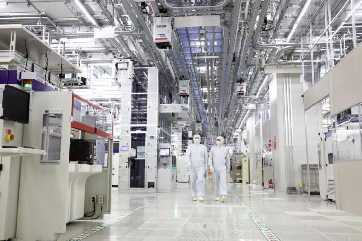
[Asia Economy Reporter Park Sun-mi] The length of a single semiconductor production line (P3) is 700 meters, longer than laying down the Lotte World Tower (555m). This was the overwhelming impression felt while touring the Samsung Semiconductor Pyeongtaek Campus facilities. First amazed by the large scale, then once again by the concentrated cutting-edge facilities, it is a place that naturally draws exclamations due to its meticulous facilities that do not tolerate even a speck of fine dust. The Samsung Semiconductor Pyeongtaek Campus, the world's largest semiconductor production base, is gaining attention as a must-visit destination for major foreign dignitaries visiting Korea. As the atmosphere for expanding semiconductor industry investment continues, inquiries for visit approvals from countries and companies considering semiconductor collaboration with Korea are flooding in.
According to the semiconductor industry on the 16th, this week Spanish Prime Minister Pedro Sanchez and Minister of Industry Reyes Maroto will visit Korea and tour the Samsung Semiconductor Pyeongtaek Campus. Spanish media also report that the visit schedule of Prime Minister Sanchez to Korea includes a tour of Samsung Electronics' semiconductor factory, and that he plans to meet with key executives including Samsung Electronics Chairman Lee Jae-yong to discuss semiconductor collaboration issues.
The Spanish government established a 12 billion euro (16 trillion won) fund in May to foster the semiconductor industry and is currently seeking investment companies to build semiconductor factories locally. The plan is to attract facilities that mass-produce advanced semiconductors below 5 nanometers. Spanish media interpret this schedule as showing that Spain regards Samsung Electronics as the most important company in semiconductor production and a benchmarking target.
The Samsung Pyeongtaek Campus has rapidly emerged as a must-visit destination for major foreign dignitaries starting this year. In 2017, during his visit to Korea, then U.S. President Donald Trump spotted the Pyeongtaek Campus while traveling by helicopter and expressed repeated amazement and a desire to visit, but until last year, no U.S. president had visited a Korean semiconductor factory. In the past, the Giheung or Hwaseong campuses were considered symbols of Samsung's semiconductor factories.
However, in May this year, as soon as U.S. President Joe Biden visited Korea, he visited the Pyeongtaek Campus together with President Yoon Suk-yeol, sharply increasing interest in the Pyeongtaek Campus. President Biden, who was focusing on expanding domestic semiconductor investment, was the first U.S. president to visit a Korean semiconductor factory, strengthening the Korea-U.S. semiconductor alliance and attracting global attention. At that time, President Biden, after touring the Samsung semiconductor factory, mentioned that Samsung's technological innovation was remarkable and said that the productive partnership between Korea and the U.S. would be strengthened in the future.
On the 5th of this month, German President Frank-Walter Steinmeier visited the Samsung Electronics Pyeongtaek Campus along with members of the German Bundestag and business figures. Germany is also actively fostering the semiconductor industry and urgently needs semiconductor cooperation with Korea. Infineon, a German representative semiconductor company, has strengths in automotive semiconductors. After touring the factory, the German president, like President Biden, left his signature not in the guestbook but on a semiconductor wafer.
The Pyeongtaek Campus boasts the world's largest scale among single semiconductor production lines equipped with cutting-edge facilities. It covers an area equivalent to 400 soccer fields (2.89 million square meters) and houses Samsung Electronics' main next-generation memory semiconductors (DRAM and NAND) and foundry (semiconductor contract manufacturing) processes. Currently, lines 1 to 3 are operational at the Pyeongtaek factory, and line 4 is undergoing site preparation for construction.
In the semiconductor industry, the Samsung Electronics Pyeongtaek factory is considered a place that countries and companies aiming to grow the semiconductor industry cannot help but be interested in, as it is the largest single semiconductor production line in the world and houses cutting-edge facilities. Even looking at line 1 alone, which involved an investment of over 30 trillion won, one can gauge the semiconductor production capacity within the Pyeongtaek factory through its equipment and layout, and by observing the construction progress of line 4, one can understand Korea's current position in semiconductors.
An industry insider explained, "In the past, requests to tour Samsung semiconductor factories mainly came from domestic politicians, but since President Biden's visit, it has become the top corporate tour destination that foreign heads of state must visit when they come to Korea," adding, "Because the strengths of Korea's semiconductor industry are clear, an atmosphere has formed overseas to benchmark it for industrial expansion."
© The Asia Business Daily(www.asiae.co.kr). All rights reserved.
![Clutching a Stolen Dior Bag, Saying "I Hate Being Poor but Real"... The Grotesque Con of a "Human Knockoff" [Slate]](https://cwcontent.asiae.co.kr/asiaresize/183/2026021902243444107_1771435474.jpg)


