A technology has been developed that enables the fabrication of flexible electronic skin without using a cleanroom. This technology is expected to enhance the practicality of electronic skin applicable to robots and wearable devices.
The Electronics and Telecommunications Research Institute (ETRI) announced on the 24th that, together with Professor Ahn Joonseong's research team in the Department of Control and Instrumentation Engineering at Korea University Sejong Campus, it has developed an in-situ process-based electronic skin fabrication technology that can produce large-area multimodal sensors without relying on a semiconductor cleanroom facility.
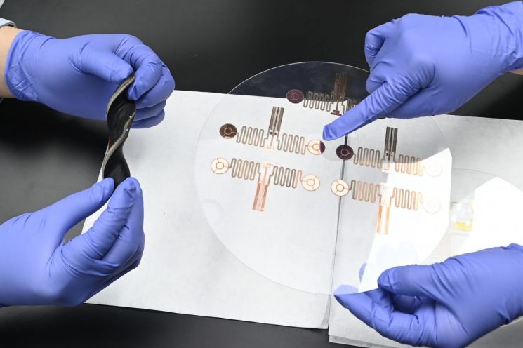 Electronic skin fabricated by a joint research team using an in-situ process. Electronics and Telecommunications Research Institute
Electronic skin is a thin, flexible sensor that detects pressure and contact, similar to human skin. It is regarded as a core technology for realizing precise tactile sensing in intelligent robots.
However, conventional flexible electronic sensors require semiconductor manufacturing processes such as photomask processes, vacuum deposition, and etching, making expensive cleanroom facilities indispensable. Because the fabrication process is complex and costly, they have had low competitiveness in terms of practicality.
When attaching tactile sensors over a large surface, such as on humanoid robots with human-like forms, there has also been the challenge of securing both process stability and reliability.
To solve these problems, the joint research team devised a maskless in-situ process technology that enables sensor fabrication without a photomask process by using a UV laser and a 3D printer. This technology is designed to fabricate sensors directly at the required locations without separate photomasks.
Through this approach, it has become possible to implement large-area capacitive flexible tactile sensor arrays based on microporous dielectrics in a short time with high reproducibility. In addition, by drastically simplifying the process steps, the team improved fabrication efficiency while reducing dependence on expensive cleanroom facilities, thereby achieving both application-specific scalability and productivity.
This technology is drawing attention because it reduces the burden of the fabrication process while providing a manufacturing environment that can be applied to various interactive systems, including intelligent robot tactile systems, human-machine interfaces (HMI), and wearable devices.
Above all, by simultaneously enabling cost reduction and rapid prototyping, it offers the advantage of responding quickly to diverse application environments such as robots, Internet of Things (IoT) devices, and healthcare.
ETRI went beyond the sensor-device level to implement up to the system level, demonstrating the feasibility of applying the technology in real robot and human-machine interface environments. Through this, it has been evaluated as having laid the groundwork for the commercialization of next-generation intelligent robot tactile systems and interactive electronic skin technologies.
Kim Hyejin, principal researcher at ETRI, said, "Electronic skin technology based on in-situ processes is a key technology that lowers the entry barrier for large-area flexible sensor fabrication while enhancing the potential for realizing interaction technologies between robots and humans," adding, "We expect it to be applicable across intelligent robots, wearable devices, and interactive systems in the future."
Meanwhile, the research results (paper) were recently published in npj Flexible Electronics, a Nature Partner Journal specializing in flexible electronic devices.
© The Asia Business Daily(www.asiae.co.kr). All rights reserved.
![Clutching a Stolen Dior Bag, Saying "I Hate Being Poor but Real"... The Grotesque Con of a "Human Knockoff" [Slate]](https://cwcontent.asiae.co.kr/asiaresize/183/2026021902243444107_1771435474.jpg)


