Nano Integrated Technology Institute and Korean Society of Microelectronics and Packaging Sign Cooperation MOU
Strengthening R&D and Industrial Competitiveness by Training Specialized Professionals
Active Utilization of 300 mm Wafer Equipment Planned
Research institutions and academia have joined forces to secure competitiveness in advanced packaging technologies that determine the performance of high-bandwidth memory (HBM), a core component of artificial intelligence (AI) semiconductors.
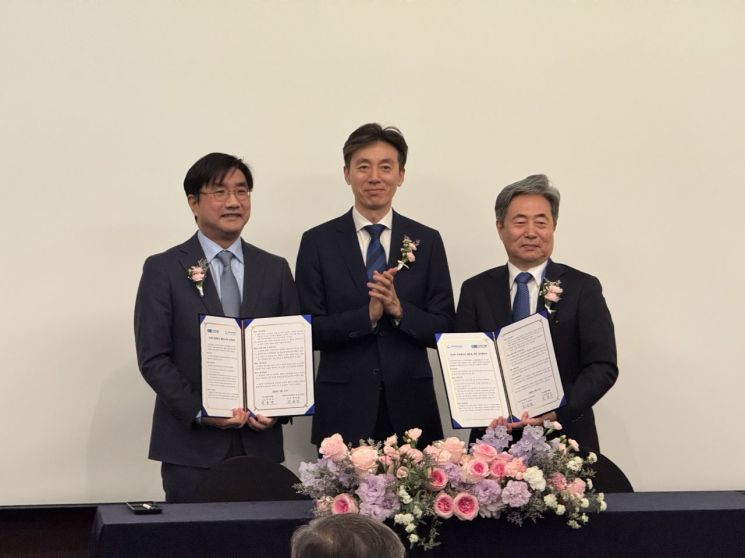 Nano Integrated Technology Institute, a public semiconductor fab under the Ministry of Science and ICT, and the Korean Society for Microelectronics and Packaging signed a strategic Memorandum of Understanding (MOU) on the 11th at the Novotel Ambassador in Gangnam, Seoul to develop advanced packaging professionals. From left: Joo Youngchang, President of the Society; Lee Gangwoo, Section Chief at the Ministry of Science and ICT; Park Heungsu, Director of the Nano Integrated Technology Institute. Photo by Paek Jongmin, Tech Specialist
The Nano Integrated Technology Institute, a public semiconductor fab under the Ministry of Science and ICT, and the Korean Society of Microelectronics and Packaging announced that on the 11th they signed a strategic memorandum of understanding (MOU) at the Novotel Ambassador in Gangnam, Seoul, to foster advanced packaging professionals, and that they will begin full-scale talent development efforts.
The event was attended by Joo Youngchang, President of the Korean Society of Microelectronics and Packaging; Park Heungsoo, Director of the Nano Integrated Technology Institute; Kim Hyeongho, President of the Korea Fabless Industry Association; and Kim Hyeongjun, Head of the Next-Generation Intelligent Semiconductor Business Division, along with other experts in semiconductors and packaging-related fields.
This agreement aims to resolve the shortage of talent in the packaging sector, whose technological complexity is rising in the rapidly growing AI semiconductor market. To that end, the Nano Integrated Technology Institute, the only public semiconductor fab in Korea, and the Korean Society of Microelectronics and Packaging, the top expert group in this field, have established a direct cooperation framework, enabling the combination of the Institute's hardware with the Society's expert know-how.
Through this agreement, the two organizations decided to focus not only on building equipment and providing basic education, but also on nurturing "field-ready engineers" who can be deployed immediately in industrial settings. To this end, they plan to use the advanced packaging batch-process equipment based on 12-inch wafers installed at the Institute to train 80 professionals per year. Trainees will gain hands-on experience with key HBM manufacturing technologies such as through-silicon via (TSV) and redistribution layer (RDL) interposer processes, thereby developing on-site capabilities. The Nano Integrated Technology Institute also plans to actively deploy packaging-related equipment to fully support workforce development.
Joo Youngchang, President of the Korean Society of Microelectronics and Packaging, said, "Packaging technology professionals can only be trained at facilities capable of handling 300 mm wafers. That is why the Nano Integrated Technology Institute is the optimal partner. By utilizing the Institute's 300 mm equipment, we can cultivate talent across a wide range of fields, including materials and machinery required for packaging."
Park Heungsoo, Director of the Nano Integrated Technology Institute, emphasized, "Through cooperation with the Society, the Institute will fully play its role in fostering field-ready talent that will lead the ecosystem of Korea's next-generation semiconductor industry."
To strengthen the domestic advanced packaging ecosystem, the Ministry of Science and ICT has been investing a total budget of 49.5 billion won since 2024 to support the establishment of advanced packaging equipment and process technologies.
Lee Kangwoo, Director of Fundamental Technology at the Ministry of Science and ICT, said, "This collaboration model, which combines the advanced packaging testbed infrastructure built with government investment and the human expertise of the Korean Society of Microelectronics and Packaging, will play an important role in enhancing Korea's global competitiveness in the semiconductor back-end process sector."
© The Asia Business Daily(www.asiae.co.kr). All rights reserved.
![Clutching a Stolen Dior Bag, Saying "I Hate Being Poor but Real"... The Grotesque Con of a "Human Knockoff" [Slate]](https://cwcontent.asiae.co.kr/asiaresize/183/2026021902243444107_1771435474.jpg)


