UNIST Team Led by Kim Jeonghwan and Jung Changwook Identifies Cause of Up to 30-Fold Overestimation in Charge Mobility
Fringe Current Induced by Electrode Geometry Found Responsible;
Device Design Standard Proposed and Published in ACS Nano
It has been revealed that there are serious errors hidden within the performance evaluation metrics that have served as a compass for researchers in the semiconductor development process.
The team led by Professors Kim Jeonghwan and Jung Changwook at the Graduate School of Semiconductor Materials and Components at UNIST announced on November 3 that the key performance metric for semiconductor devices, known as 'Field-Effect Mobility,' can be measured up to 30 times higher than its actual value depending on the device structure. The team also proposed a standard for semiconductor device structural design to address this issue.
 Research team (from left) Professor Kim Jeonghwan, Professor Jung Changwook, Researcher Kim Suhyun (first author), Researcher Lee Youngjun (first author). Provided by UNIST
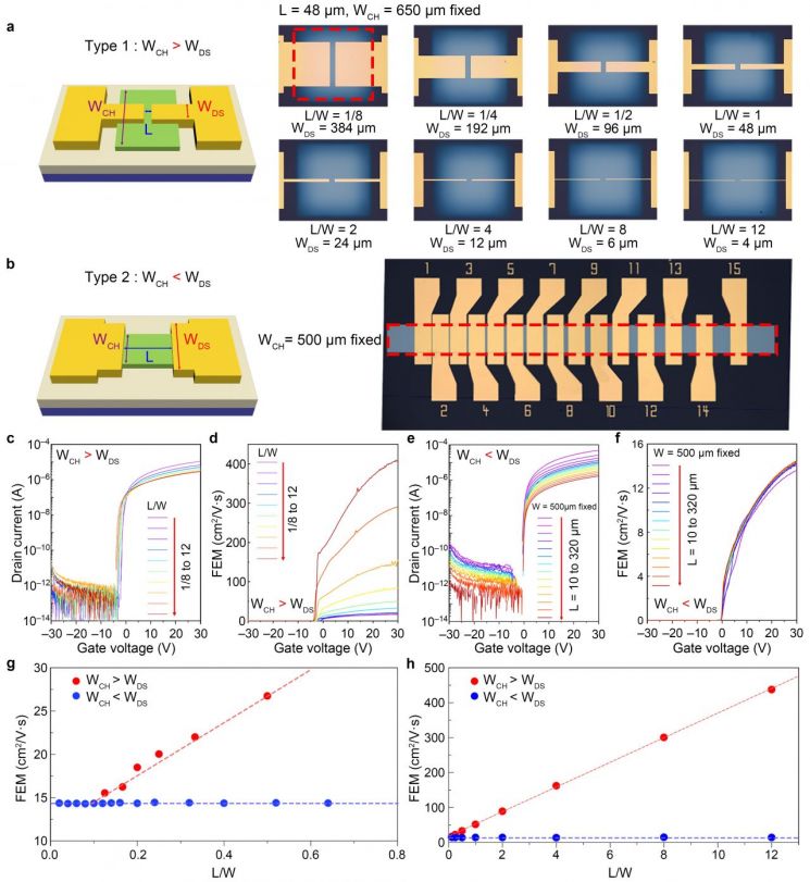
Charge mobility is an indicator of how quickly and efficiently charges (current) move inside a semiconductor. The higher this value, the faster the device operates and the lower its power consumption, making it a critical metric for determining the success of high-performance semiconductor chip development.
According to the research, this charge mobility can be overestimated by more than 30 times depending on the geometric structure of oxide thin-film transistor semiconductor devices.
The research team identified 'fringe current'-current that flows along unintended paths-as the cause. In thin-film transistor devices, current enters through the 'source electrode,' travels through the main path called the 'channel,' and exits via the 'drain electrode.' However, if the channel width is much larger than the electrode, a 'fringe current' arises, where current spreads and flows not only through the intended path directly beneath the electrode but also through the wide surrounding area outside the electrode. Since measurement equipment sums up all these currents to calculate performance, the results are inflated beyond the actual value.
If charge mobility is likened to the average speed of cars on a congested highway, fringe current is akin to including cars speeding along the shoulder, making the overall average speed appear much higher than it truly is.
The research team also presented a design standard for thin-film transistor devices to resolve this issue. They recommended designing the channel width to be narrower than the electrode width, or, if unavoidable, ensuring that the electrode width is at least 12 times greater than the total device length (L/W ≤ 1/12).
Experiments and simulations demonstrated that following this standard almost completely eliminates the effect of fringe current, resulting in no difference between the actual and measured mobility, and enabling accurate performance measurement.
The team further recommended measuring the Hall mobility alongside the field-effect mobility for cross-verification. Hall mobility measures the intrinsic electrical properties of the semiconductor thin-film material itself, rather than the completed device, and is thus free from errors caused by the geometric structure of the semiconductor device.
Professor Kim Jeonghwan stated, "Errors in device performance measurement can lead to the misidentification of overestimated materials as promising next-generation technologies, wasting research capacity, or make objective technology comparisons impossible, thereby hindering the overall advancement of the semiconductor industry. This research is significant in that it proposes a global standard to resolve these issues."
This research was published on October 21 in ACS Nano, a nanoscience journal issued by the American Chemical Society.
The study was supported by the National Research Foundation of Korea under the Ministry of Science and ICT, as well as the Ministry of Trade, Industry and Energy.
© The Asia Business Daily(www.asiae.co.kr). All rights reserved.

![User Who Sold Erroneously Deposited Bitcoins to Repay Debt and Fund Entertainment... What Did the Supreme Court Decide in 2021? [Legal Issue Check]](https://cwcontent.asiae.co.kr/asiaresize/183/2026020910431234020_1770601391.png)


