Located near Honmachi, Osaka, Japan
Optimal for office operations with many nearby subway stations
'Horizontal structure' offices popular in Japan draw attention
Office environment breaking down ranks seems to have won over TSMC
Japan's plant construction capability also stands out
Kumamoto TSMC Plant 1 completed in just two years
Relaxed construction regulations and government support also play a role
TSMC, the world’s leading foundry (semiconductor contract manufacturing) company based in Taiwan, has been strengthening its ties with Japan as much as with the United States in recent years. The goals and plans that TSMC aims to achieve in Japan, in terms of importance, value, and scale, are by no means inferior to the $100 billion (approximately 146 trillion won) investment plan in the United States that was announced at the White House in March.
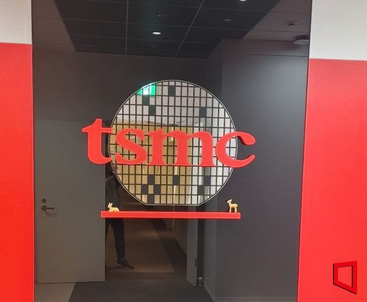 When entering the TSMC Design Center office in Osaka, Japan, the TSMC logo is the first thing you see straight ahead. Photo by Kim Hyungmin
According to foreign media and industry sources on May 15, TSMC is in the process of taking steps to build additional foundry plants and design centers in Japan. The first plant in Kumamoto was completed in February last year and has begun mass production of semiconductors, while a second plant is under construction in the same area. The goal is to have the second plant operational by 2027. Meanwhile, discussions are underway with the Japanese government about the possibility of building a third plant in Osaka. TSMC is also searching for a suitable location to establish another design center in addition to those already in Yokohama and Osaka. TSMC has officially stated, "Our plans in Japan will not be neglected due to our investment in the United States. We will proceed as planned."
What makes Japan so attractive to TSMC? The answer became clear after visiting the TSMC Design Center in Osaka and listening to explanations from local officials. The reasons TSMC has chosen Japan as a key production base include a flexible business environment and rapid, precise construction capabilities.
'Horizontal Structure' Offices That Won TSMC's Heart
The TSMC Osaka Design Center is located near Honmachi, an area densely packed with various company offices. It is about a 20-minute walk from Oebashi subway station. In addition to Oebashi, there are many other nearby subway stations such as Yodoyabashi, Higobashi, and Honmachi, making it an optimal location for business visitors. The design center is on the 13th floor of the Obic Midosuji Building. The building rents office spaces to companies, and TSMC appears to occupy the largest space. The office atmosphere was generally quiet, with Japanese employees working diligently. Upon entering the office, a large TSMC logo greets visitors, and to the right, wall clocks display the local times in major cities in Taiwan, Japan, the United States, and the Netherlands. This seems to reflect TSMC’s commitment to producing custom chips in line with clients’ time zones. As expected from TSMC, which is known for its strict protection of trade secrets, there was also a notice stating, "Photography is strictly prohibited here." A Japanese TSMC employee added, "It is difficult to provide any information without prior approval from our Taiwan headquarters."
However, what could be observed over the employee’s shoulder was the ‘horizontal structure’ of the office. All employees, regardless of rank, had workspaces of the same location and height. According to local officials, most company offices in Japan are designed this way. It can be seen as a uniquely Japanese office structure. When constructing buildings, Japan often uses a horizontal structure that shares a wall with the neighboring unit, allowing for immediate evacuation in case of earthquakes or fires. This architectural approach appears to have been adopted in office design as well. It is reportedly so popular that many companies are applying it when building new offices.
This structure is ideal for companies that aim to foster a team-oriented atmosphere rather than management driven by executive leadership. It has also won over global companies. General Motors (GM), Ford, and Motorola are said to have adopted horizontal office layouts in their Japanese offices. TSMC appears to have done the same. The design center is where TSMC communicates and coordinates processing methods and designs before producing chips tailored to customer requirements. It is the ‘starting point’ for custom chip production. To gather many ideas and find the optimal production method, TSMC likely saw the unique horizontal structure of Japanese offices as a good fit.
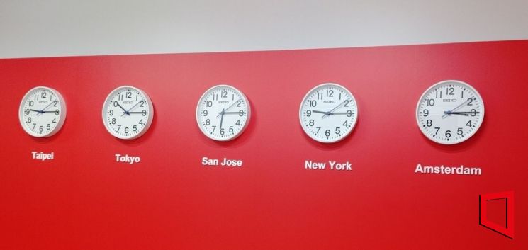 On one wall of the TSMC Design Center in Osaka, Japan, wall clocks indicating the local times of major cities where clients from Japan, the United States, the Netherlands, and other countries are located are hung. Photo by Kim Hyungmin
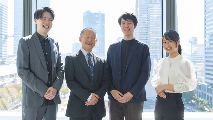 Takuya Yasui (center left in the photo), who serves as the head of the Japan Design Center at TSMC Design Technology Japan, along with employees. Photo by TSMC Design Technology Japan website
Building a Plant in Just Two Years
Another reason frequently cited by local officials for TSMC’s desire to establish many production bases in Japan is the country’s ‘construction capability.’ After announcing the construction plan for the first Kumamoto plant in 2022, Japan completed it in just two years. While semiconductor plants typically take three to four years to build, Japan significantly shortened this to two years. Kang Kyungsung, president of KOTRA, noted, "This is a point we need to pay close attention to."
The flexible and open environment for plant construction in Japan is seen as a contributing factor. Japan is recognized worldwide for its exceptional capabilities in large-scale construction projects, excelling not only in buildings but also in land reclamation. In Osaka, for example, there are many landmarks built on artificial islands, such as Kansai International Airport, and Yumeshima, the site of the 2025 Osaka-Kansai Expo, is also an artificial island created through reclamation. Japanese buildings are renowned for their ‘seismic design,’ developed through extensive experience with natural disasters. Considering the need for a clean and safe environment, semiconductor plants are regarded as among the types of factories Japan is best equipped to build. Furthermore, the ability to carry out construction quickly is another reason semiconductor companies, facing fierce competition and the need to establish production bases rapidly, are turning to Japan.
Japan’s recent significant easing of location regulations for semiconductor plants has also attracted TSMC. According to a KOTRA report, in October 2023, the Japanese government amended laws and regulations to allow semiconductor construction even in ‘urbanization control areas,’ where local governments had previously restricted development of farmland and forests. Additionally, the Japanese government’s broad support and the yen exchange rate are seen as factors that facilitated TSMC’s plant construction. In June 2022, the Japanese government passed a subsidy bill for TSMC’s Kumamoto plant, providing 476 billion yen (about 4 trillion won) for the first plant and 730 billion yen (about 7 trillion won) for the second plant. TSMC entrusted the construction of the Kumamoto plant to Kajima Corporation, a Japanese construction company. During the construction period, the weak yen allowed TSMC to offer wages higher than the local average, which reportedly boosted worker motivation on site.
© The Asia Business Daily(www.asiae.co.kr). All rights reserved.


