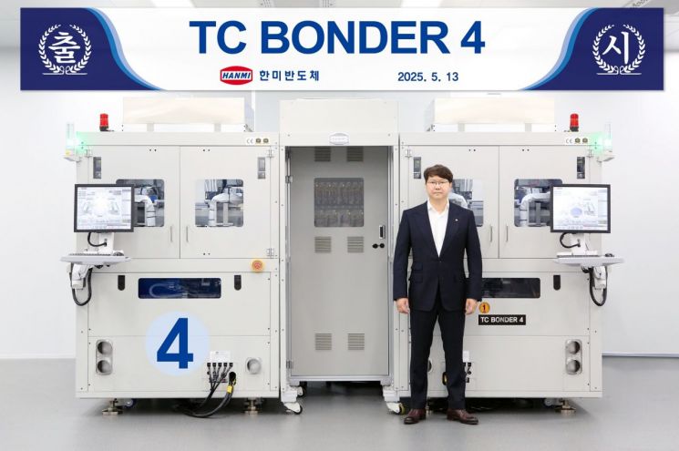
Hanmi Semiconductor announced on May 14 that it will launch the 'TC Bonder 4 (TC BONDER 4),' a dedicated piece of equipment for producing HBM4, which is a core component of next-generation AI semiconductors.
Kwak Dongshin, Chairman of Hanmi Semiconductor, stated, "With the rapid growth of the AI market, the global HBM market is experiencing explosive growth every year," and added, "Nvidia's next-generation product, Blackwell Ultra, which will be introduced in the second half of this year, will also be produced using Hanmi Semiconductor's TC Bonder." He continued, "Hanmi Semiconductor's number one global market share and competitiveness in HBM TC Bonders remain unchanged."
Some in the industry have suggested that hybrid bonding technology is necessary for HBM4 production. Last month, after the international semiconductor standards organization JEDEC relaxed the standard height for HBM4 to 775 micrometers (μm), Hanmi Semiconductor was expected to directly benefit, as its TC Bonder equipment would now be capable of manufacturing HBM4.
Chairman Kwak introduced, "TC Bonder 4 is a dedicated piece of equipment capable of producing HBM4, and it features significantly improved productivity and precision compared to competitors, tailored to the highly sophisticated precision required by HBM4." He added, "As global semiconductor customers actively use it for HBM4 production, it will make a significant contribution to sales as the HBM4 market expands in the future."
Memory companies worldwide are preparing for mass production of HBM4 in the second half of this year. HBM4, the sixth-generation high-bandwidth memory, boasts innovative performance, with speed improved by 60% and power consumption reduced to 70% compared to the previous fifth generation (HBM3E). It supports up to 16 layers, and the capacity per DRAM has expanded from 24Gb to 32Gb. The number of silicon via (TSV) interfaces, which serve as data transmission channels, has doubled to 2,048 compared to the previous generation, increasing data transfer speeds between the processor and memory.
As the stacking process for HBM with 16 layers or more requires extremely high precision, the importance of advanced bonding technology is growing, and Hanmi Semiconductor's TC Bonder is expected to play a decisive role in determining the completeness of HBM stacking.
Founded in 1980, Hanmi Semiconductor is a global semiconductor equipment company with approximately 320 customers worldwide. Since establishing its Intellectual Property Department in 2002, the company has focused on protecting and strengthening its intellectual property rights, having filed a total of around 120 patents related to HBM equipment to date.
Currently, Hanmi Semiconductor holds a market share of over 90% in the TC Bonder market for 12-layer HBM3E production, demonstrating its unrivaled technological capability. With the launch of this dedicated HBM4 equipment, the company is expected to further strengthen its position in the global AI semiconductor market.
© The Asia Business Daily(www.asiae.co.kr). All rights reserved.
![Clutching a Stolen Dior Bag, Saying "I Hate Being Poor but Real"... The Grotesque Con of a "Human Knockoff" [Slate]](https://cwcontent.asiae.co.kr/asiaresize/183/2026021902243444107_1771435474.jpg)


