Memories of Survival Amid Chaos
Development of HBM Packaging Technology
Electronics Manufacturing Technology Award and Kang Daewon Award
Lee Kang-wook, Vice President in charge of Advanced Packaging Development at SK Hynix, recalled the day 14 years ago that put him at the crossroads of life and death on the 11th. At 2:46 p.m. on March 11, 2011, a massive earthquake with a magnitude of 9.0 on the Richter scale, the largest ever recorded by Japanese observation, struck the Tohoku region of Sendai City, Miyagi Prefecture, Japan. At that time, Vice President Lee was a professor teaching students at Tohoku University and experienced the terror of the earthquake firsthand.
The memory of that day remains vivid for him. He says he feels both relief at having survived the disaster and deep gratitude for his current life. He also holds a heartfelt remembrance for those who suffered and sacrificed due to the earthquake. In a phone interview with Asia Economy on the 13th, Vice President Lee calmly recalled, "I believe I exist now because I survived that day."
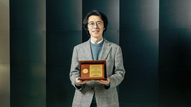 Lee Kang-wook, Vice President of SK Hynix, who received the Kang Dae-won Award last February. Photo by SK Hynix Newsroom
The experience of crossing the threshold of survival seems to have made Vice President Lee even stronger. After gaining recognition for his research achievements while working a bit longer at Tohoku University in Japan, he joined SK Hynix in 2018 and led the development of packaging technology required for high-bandwidth memory (HBM) products as the person in charge of wafer-level packaging (WLP) development.
In particular, Vice President Lee played a crucial role in SK Hynix gaining an edge in the HBM market by successfully introducing an innovative technology called MR-MUF (a process technology that injects and solidifies a liquid protective material between stacked semiconductor chips to protect the circuits between chips) during the development of the third-generation HBM product, HBM2E, in 2019. This technology is proudly unique to SK Hynix and has enabled the company to aim for the highest tiers of HBM3E and HBM4.
Recognized for these achievements, Vice President Lee swept important awards in academia. In May last year, he became the first Korean to receive the Electronics Manufacturing Technology Award from the Electronic Packaging Society (EPS) under the Institute of Electrical and Electronics Engineers (IEEE), the most prestigious organization in the global electrical and electronics engineering field. In February this year, he was selected as the recipient of the 8th Kang Dae-won Award at the 32nd Korea Semiconductor Conference held in Jeongseon, Gangwon Province.
This award was established to honor the achievements of the late Dr. Kang Dae-won, who left a monumental legacy in the semiconductor industry. According to SK Hynix, Vice President Lee is the first entrepreneur in the semiconductor post-processing packaging field to receive this award. Posting a photo holding the Kang Dae-won Award plaque as his main profile picture on his smartphone messenger, he said, "All the awards I have received are meaningful, but the Kang Dae-won Award holds a bit more significance."
What will be Vice President Lee’s next move? While he was reserved about his next project, he said, "I am diligently researching and developing technology in line with the company’s goals." Reflecting on his previous statements emphasizing that "packaging technology can determine the survival of semiconductor companies," it seems that Vice President Lee’s eyes and ears are focused on developing new packaging technologies.
© The Asia Business Daily(www.asiae.co.kr). All rights reserved.


