Suppressing the Effects of Space Radiation
on Nano-Semiconductor Surfaces
with a Thin Passivation Layer
Domestic researchers have developed semiconductor radiation-hardening technology against protons, which account for more than 80% of space radiation.
There are many types of radiation in space, which cause over 30% of product failures using semiconductors. Therefore, radiation-hardening technology that can withstand radiation is very important for the development of next-generation aerospace semiconductors.
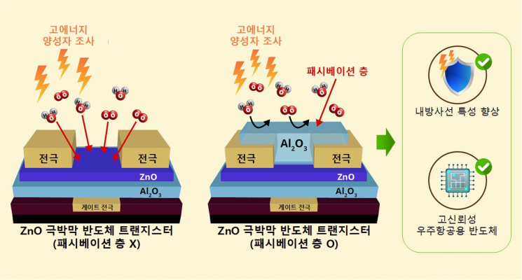 Schematic diagram of radiation shielding technology for aerospace nano semiconductors. Provided by Korea Atomic Energy Research Institute
The Advanced Radiation Research Institute of the Korea Atomic Energy Research Institute (KAERI) announced on the 6th that, through joint research with Pohang University of Science and Technology (POSTECH), they succeeded in developing radiation-hardening technology that significantly suppresses nano-semiconductor errors caused by protons by physically separating the semiconductor surface from the outside and stacking a passivation layer that blocks water and oxygen in the atmosphere.
Dr. Changgu Kang’s radiation fusion research team at KAERI and Professor Byunghoon Lee’s team at POSTECH utilized an atomic layer deposition method, which creates a gaseous state of material and deposits it thinly on the surface through chemical reactions, to stack a 10 nm thick aluminum oxide (Al2O3) passivation layer on the surface of zinc oxide (ZnO)-based nano-semiconductors.
After irradiating both semiconductors with and without the passivation layer using a proton accelerator and comparing the changes in electrical characteristics, it was confirmed that the passivation layer very effectively suppresses changes in the electrical characteristics of semiconductors exposed to protons.
Semiconductors protected by the passivation layer showed a 60% reduction in threshold voltage change and about a 90% reduction in hysteresis index and stress index changes compared to unprotected semiconductors after proton irradiation. In particular, the noise value did not change at all even after proton exposure.
 From the left, Dr. Yongsoo Lee, Korea Atomic Energy Research Institute (first author), Dr. Changgu Kang, Korea Atomic Energy Research Institute (corresponding author), and Professor Byunghoon Lee, Pohang University of Science and Technology (corresponding author). Provided by Korea Atomic Energy Research Institute.
This technology is expected to become a core technology for implementing radiation-hardening systems for next-generation aerospace nano-semiconductors by effectively protecting semiconductors from the effects of protons, which constitute most of space radiation.
Jung Byung-yeop, director of the Advanced Radiation Research Institute at KAERI, said, "This technology is a case where a passivation layer was deposited on next-generation nano-semiconductors using atomic layer deposition and the actual radiation-hardening effect was verified," adding, "We will make further efforts to secure a competitive edge in aerospace semiconductor technology for South Korea."
In this study, KAERI was responsible for semiconductor fabrication and proton irradiation experiments, while POSTECH handled the analysis of electrical characteristic changes. The research results were published in the January issue of the international journal Nano Convergence. (Paper title: Enhanced high-energy proton radiation hardness of ZnO thin-film transistors with a passivation layer)
© The Asia Business Daily(www.asiae.co.kr). All rights reserved.


