A bipolar semiconductor device based on indium selenide (InSe) that delivers high performance in both N-type and P-type semiconductors has been developed in Korea.
Indium selenide (an inorganic compound composed of indium and selenium) is attracting attention as a next-generation two-dimensional layered nanomaterial due to its superior electron mobility and saturation velocity more than twice as fast as silicon semiconductors. However, it has mainly been limited to use as an N-type semiconductor. In contrast, the newly developed bipolar semiconductor device is significant because it can be applied not only to the existing N-type but also to the P-type.
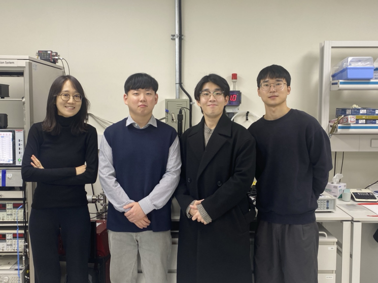 (From left) Professor Lee Gayoung, Master’s student Yeom Dongju, Integrated Master-PhD student Kim Minsu, PhD student Seok Yonguk. Provided by KAIST
KAIST announced on the 30th that Professor Gayoung Lee’s research team from the Department of Electrical Engineering developed a bipolar multifunctional transistor based on the nanosemiconductor indium selenide.
Indium selenide has been primarily used as an N-type semiconductor because it is difficult to induce holes (positive charge carriers necessary for implementing P-type transistors) required for P-type semiconductors and complementary circuit implementation.
However, the research team solved this problem through a new device structure design and developed a bipolar semiconductor device that can be applied to both N-type and P-type transistors.
The method involves placing electrodes beneath the indium selenide and improving the metal-semiconductor junction characteristics to realize bipolar properties where electrons and holes can selectively flow.
The bipolar semiconductor device developed by the research team recorded on/off current ratios of 10^9 (one billion) or higher for both N-type and P-type. Silicon semiconductor devices generally exhibit unipolar operation with ratios below 10^8, and there have been no reported cases of bipolar two-dimensional semiconductors capable of simultaneous N-type and P-type operation achieving on/off ratios above 10^8 for both types, according to the research team.
Professor Gayoung Lee explained, “Multifunctional devices generally require complex processes and structures, making fabrication and integration difficult. However, in this study, by introducing a partial gate structure, we fabricated a multifunctional device capable of implementing various functions in a single device, improving process efficiency and increasing flexibility in circuit design.”
Meanwhile, this research was conducted with support from the Korea Basic Science Institute National Research Facilities & Equipment Center, the National Research Foundation of Korea’s Excellent Research Program, KAIST Leap Research Program, and Samsung Electronics.
© The Asia Business Daily(www.asiae.co.kr). All rights reserved.
![Clutching a Stolen Dior Bag, Saying "I Hate Being Poor but Real"... The Grotesque Con of a "Human Knockoff" [Slate]](https://cwcontent.asiae.co.kr/asiaresize/183/2026021902243444107_1771435474.jpg)

