Chungnam Province, Cheonan City, and Samsung Electronics Sign Agreement... To Be Installed by 2027
In Cheonan, Chungnam, Samsung Electronics' state-of-the-art, large-scale semiconductor packaging process facility will be established by 2027.
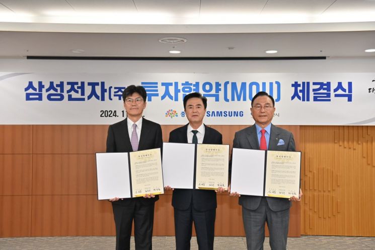
On the 12th, Governor Kim Tae-heum signed an MOU in the provincial government situation room with Samsung Electronics President Nam Seokwoo and Cheonan Mayor Park Sangdon.
Accordingly, Samsung Electronics plans to lease a building on a 280,000-square-meter site within the Samsung Display area in Cheonan's 3rd General Industrial Complex, install semiconductor packaging process facilities from next month until December 2027, and produce HBM and other products.
HBM, or High Bandwidth Memory, is an ultra-high-speed DRAM based on high bandwidth that processes massive data for AI, and is used in data centers and supercomputers.
The province expects that producing HBM at the semiconductor packaging process facility will enable it to secure leadership in the global advanced semiconductor market.
Governor Kim stated, "Coexistence between companies and the region is the core model for economic growth in Strong Chungnam, and we will communicate and cooperate with companies with the belief that Chungnam thrives when businesses thrive." He added, "We will implement business-friendly policies so that Samsung can grow and develop even further in Chungnam."
© The Asia Business Daily(www.asiae.co.kr). All rights reserved.
![Clutching a Stolen Dior Bag, Saying "I Hate Being Poor but Real"... The Grotesque Con of a "Human Knockoff" [Slate]](https://cwcontent.asiae.co.kr/asiaresize/183/2026021902243444107_1771435474.jpg)


