Addition of SF2Z and SF4U to Existing Foundry Process
Emphasizing Turnkey Competitiveness Combining Memory and Packaging
On the 12th (local time), Samsung Electronics held the 'Samsung Foundry Forum 2024' in Silicon Valley, USA, unveiling its foundry (semiconductor contract manufacturing) technology strategy to lead the artificial intelligence (AI) era.
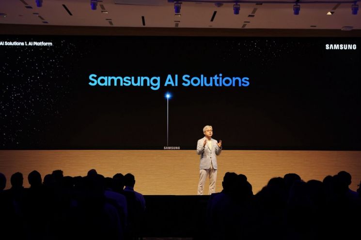 On the 12th (local time), Choi Si-young, head of Samsung Electronics' Foundry Business Division, delivered the keynote speech at the 'Samsung Foundry Forum 2024' held in Silicon Valley, USA. /
 Under the theme 'Empowering the AI Revolution,' this event presented Samsung's differentiated strategy, including cutting-edge foundry technology and synergy creation through collaboration with memory and advanced packaging sectors to realize customers' AI ideas.
Choi Si-young, President of Samsung Electronics Foundry Business, said in his keynote speech, "We will provide a one-stop AI solution that customers need in the AI era through gate-all-around (GAA) process technology optimized for AI semiconductors and optical device technology capable of high-speed data processing with low power consumption."
At the event, Samsung Electronics additionally revealed SF2Z and SF4U in its existing foundry process roadmap.
The company plans to prepare the 2-nanometer process (SF2Z) applying BSPDN (Back Side Power Delivery Network) technology by 2027. BSPDN is a technology that places current wiring layers on the wafer's backside to improve bottlenecks in power and signal lines. Another new process, the 4-nanometer SF4U, can enhance PPA (power consumption, performance, area) competitiveness through optical shrink. Mass production is scheduled for 2025.
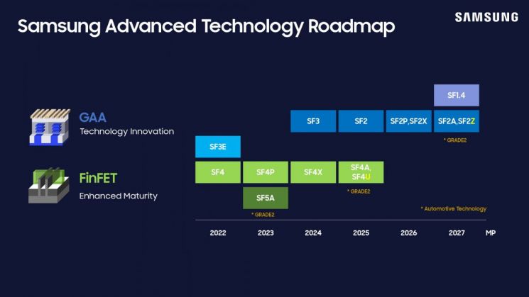
Samsung Electronics announced plans for mass production of the 1.4-nanometer process in 2027 and stated that it has secured the targeted performance and yield. In the second half of the year, it plans to start mass production of the second-generation 3-nanometer process applying GAA. The company explained that owning foundry, memory, and advanced packaging businesses is advantageous for collaboration to provide custom solutions tailored to specifications and customer demands needed in the AI era. By 2027, it plans to integrate optical devices into AI solutions as well.
On the 13th (local time), the 'SAFE (Samsung Advanced Foundry Ecosystem) Forum 2024' will be held. This year's theme is "AI: Exploring Possibilities and Future," where Samsung Electronics will create a venue to share and present customized technologies and solutions for customers in the AI era together with its partners.
© The Asia Business Daily(www.asiae.co.kr). All rights reserved.
![Clutching a Stolen Dior Bag, Saying "I Hate Being Poor but Real"... The Grotesque Con of a "Human Knockoff" [Slate]](https://cwcontent.asiae.co.kr/asiaresize/183/2026021902243444107_1771435474.jpg)


