TSMC CEO Skips Own Event → Attends ASML Event
Hears Explanation of 'Expensive' High-NA EUV
Japan's Rapidus Learns EUV Usage at US IBM
As competition in semiconductor ultra-fine process technology intensifies, foundry companies aiming for mass production of semiconductors below 2 nanometers (nm; 1 nanometer is one billionth of a meter) are accelerating efforts to secure related technologies and equipment. Taiwan's TSMC, the world's number one foundry company, had its CEO personally visit ASML to receive explanations about next-generation extreme ultraviolet (EUV) lithography equipment, while Japan-backed Rapidus dispatched 100 employees to the IBM research lab in the United States to develop advanced semiconductor technologies.
According to Digitimes and others on the 29th, Wei Zhejia, CEO of TSMC, instead of attending the 'TSMC Technology Symposium 2024' held in Taipei, Taiwan on the 23rd, visited the headquarters of Dutch semiconductor equipment company ASML and met with ASML CEO Christopher Vinke. Vinke posted on his social media, "I introduced ASML's latest technologies and new products to CEO Wei and explained how the high-NA EUV equipment implements fine process technology," along with a photo taken with him.
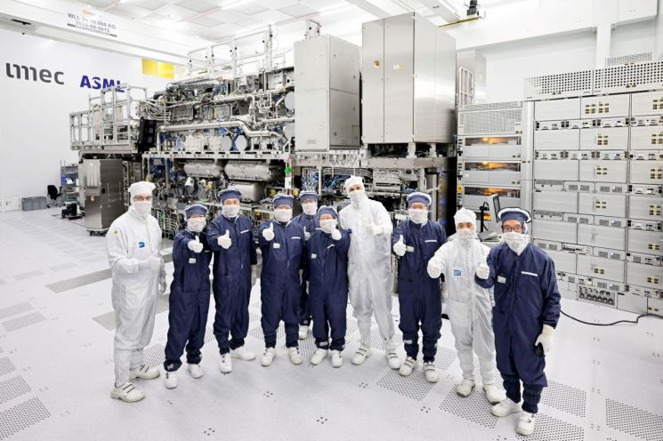 Weijia TSMC CEO and Christopher Fuque ASML CEO, among others, are taking a commemorative photo during their visit to the headquarters of Dutch semiconductor equipment company ASML. (Photo by Christopher Fuque ASML CEO SNS)
The new high-NA EUV, exclusively produced by ASML, can draw circuits more precisely than existing EUV equipment but costs more than twice as much, exceeding 500 billion won per unit. TSMC had even declared that it would handle the 2nm process using existing equipment, citing the equipment's high cost. However, it appears that TSMC has judged that investment is inevitable to firmly maintain its current dominance amid the foundry industry's technological competition over ultra-fine processes.
TSMC aims to mass-produce 2nm semiconductors by next year. It is reported that TSMC plans to produce the 1.6nm product A16, scheduled for mass production in the second half of 2026, using existing equipment and is considering introducing high-NA EUV from subsequent processes.
High-NA EUV is equipment that other foundry companies such as Samsung Electronics and Intel are also striving to acquire. Samsung Electronics Chairman Lee Jae-yong met with CEO Vinke last month to strengthen the 'semiconductor triangular alliance,' and Intel declared in March that it is stabilizing high-NA EUV equipment faster than expected and has advanced the timeline for deploying it in production lines to next year.
Japan's Rapidus Dispatches 100 Employees to IBM Research Lab
In addition to securing advanced equipment, semiconductor companies are also focusing on technology development for mass production of 2nm semiconductors. The Japanese Nihon Keizai Shimbun recently reported that about 100 Rapidus employees are concentrating on 2nm semiconductor technology development at the IBM research lab located in Albany, New York, USA. This reflects Japan's goal to produce 2nm semiconductors domestically by 2027 while actively utilizing American technology.
The Albany IBM research lab is located about a three-hour drive from New York City and covers an area three times the size of the Tokyo Dome. It is the largest in the United States based on 12-inch (300mm) wafer fabs. Nihon Keizai explained that the IBM lab was the first in the world to succeed in designing and developing 2nm semiconductors and that although the lab is a research and development hub, its interior is constructed in the form of a semiconductor factory.
The core task of Rapidus engineers at the IBM lab is developing mass production technology for 2nm semiconductors. Rapidus has set a goal to have the capability to mass-produce 2nm semiconductors at a factory under construction in Hokkaido, Japan, by 2027. To this end, Rapidus engineers are learning how to use EUV equipment from IBM engineers.
Since Japan is targeting not only advanced semiconductor production technology development but also mass production, the IBM lab is also focusing on identifying potential issues that may arise during the mass production process. Because various causes can reduce production yield?from contamination during semiconductor manufacturing to issues in production processes or design?the Albany lab has established a simulated production line to find solutions whenever problems occur.
To learn IBM Research's technology, seven Rapidus engineers were first dispatched in April last year. Rapidus plans to expand the number of dispatched personnel to 200. Nihon Keizai reported that half of the engineers are responsible for production processes, while the rest are device engineers who measure and analyze performance and design engineers who work on circuit design. It is known that they are currently researching over 300 topics.
Mukesh Kare, head of semiconductors at IBM Research, said, "Because competition is fierce, product development with an eye on post-2027, when Rapidus will start mass production, is important."
© The Asia Business Daily(www.asiae.co.kr). All rights reserved.
![Clutching a Stolen Dior Bag, Saying "I Hate Being Poor but Real"... The Grotesque Con of a "Human Knockoff" [Slate]](https://cwcontent.asiae.co.kr/asiaresize/183/2026021902243444107_1771435474.jpg)


