Pat Gelsinger's Remarks in Interview with Bloomberg
US Ohio Plant Could Become World's Largest
Full Effort to Pass Semiconductor Act and Secure ASML Equipment
Pat Gelsinger, CEO of Intel, a leading American semiconductor company, emphasized that the establishment of the foundry (semiconductor contract manufacturing) business is crucial not only for Intel but also for the future of the nation. After deciding to re-enter the foundry business immediately upon his appointment in 2021, he has been fully dedicated to building and expanding the business throughout his three-year term. His public efforts to persuade lawmakers during the creation of the U.S. CHIPS Act and his aggressive lobbying of ASML, a powerful Dutch semiconductor equipment company often called a 'super subcontractor,' right after taking office, are seen as driven by more than just business interests?they reflect genuine commitment.
In an interview with Bloomberg Businessweek released on the 1st (local time), Gelsinger said that Intel’s Ohio foundry complex could become the largest in the world, adding, "Semiconductors are essential for our economy and national security. Failure is not an option." The Ohio plant is the core headquarters of the foundry business that Gelsinger is driving forward.
Bloomberg Businessweek reported in an article titled "Intel Inside Ohio" that the construction of the Ohio plant is accelerating, alongside Gelsinger’s interview. In 2022, Gelsinger decided to invest $20 billion (approximately 27.6 trillion KRW) to build a foundry plant in Ohio. Although the initial goal was mass production by 2025, there are now expectations that construction will continue until the end of 2026.
During the construction of the Ohio plant, Gelsinger supported the Biden administration’s push for the CHIPS Act. He publicly warned that the U.S. could lose a leading semiconductor company if funding was not increased. Recalling the situation in the Bloomberg interview, he said, "I had to choose between passing the CHIPS Act or deciding to build all factories in Asia."
As a result, in March, the Biden administration announced a total support package of $19.5 billion for Intel, including $8.5 billion in subsidies and up to $11 billion in loans. This was the largest support amount decided based on the U.S. CHIPS Act. Intel is currently building two factories on the Ohio site, but considering the size of the land, it has left open the possibility of expanding to up to eight factories. Intel also revealed plans to invest up to $100 billion in total to build a manufacturing complex there.
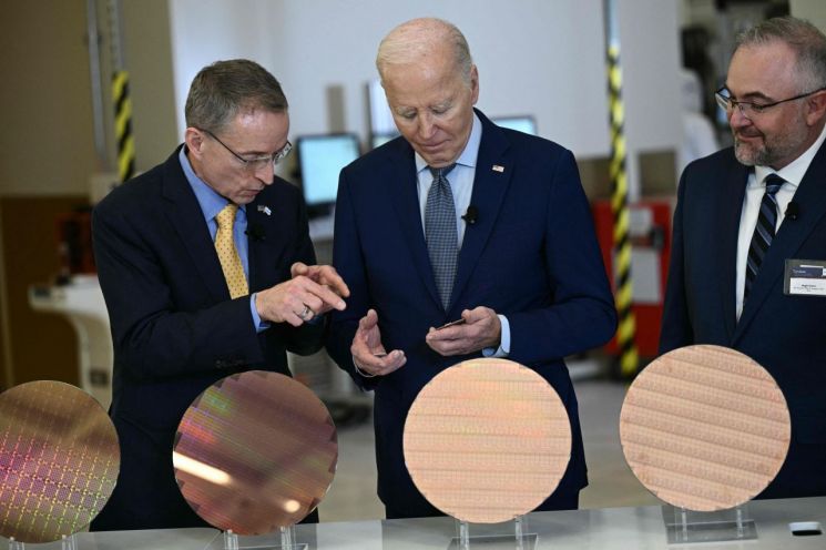 Pat Gelsinger, Intel CEO (far left), is explaining semiconductor-related matters to U.S. President Joe Biden (center), who visited Intel's Arizona campus last March.
 [Image source=AFP Yonhap News]
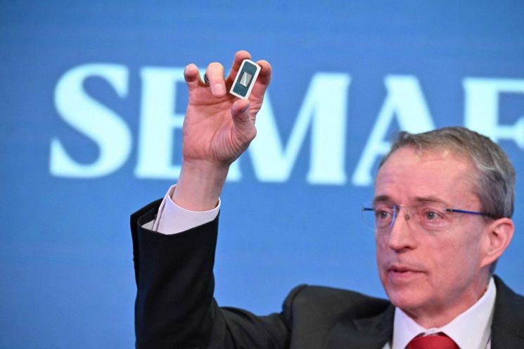
In the foundry industry, what is essential for producing cutting-edge semiconductors is not only funding and land for factory construction. Securing extreme ultraviolet (EUV) lithography equipment, which is indispensable for advanced semiconductor production, is also critical. Gelsinger revealed that he began aggressive lobbying of ASML immediately after taking office. He recalled, "It was like saying, 'We will neither debate this nor end the meeting, and you cannot leave the room.'"
Through this, Intel was able to be the first to introduce the next-generation lithography equipment called 'High NA EUV,' which can draw semiconductor circuits more precisely. Gelsinger explained, "25% of the investment in the Ohio plant goes to building construction, and 75% goes to equipment purchases." Besides securing equipment, Intel is also focusing on building essential infrastructure for semiconductor factories, such as land, power, and water supply. Bloomberg also reported that Intel is constructing roads to facilitate transportation and is actively recruiting engineers.
The reason Gelsinger is so passionate about the foundry business is that he believes it is Intel’s future. When he declared Intel’s re-entry into the foundry business in 2021, he even vowed to "lead Intel’s revival." Intel had previously entered the foundry business in 2016 but withdrew after two years.
Gelsinger, who started working at Intel at age 18, was mentioned as a leading candidate for CEO in 2006 when he was senior vice president but left Intel in 2009 after being excluded from personnel decisions. After his departure, Intel, along with ASML, began developing EUV technology, but the management at the time decided to use existing equipment due to the enormous costs and withdrew from the EUV development process. Gelsinger described this as "one of the most foolish decisions Intel ever made" in the interview.
At that time, Gelsinger was CEO of VMware and recalled that Intel was on the verge of complete collapse and "no one could have saved it." Unable to stand by, despite being an outsider as VMware CEO, he sent a letter directly to Intel’s board urging radical strategy changes. He declared his intention to invest billions of dollars in fab construction to catch up with TSMC’s cutting-edge semiconductor manufacturing processes and to enter the foundry business. That is how he returned to Intel.
Gelsinger emphasized, "In the semiconductor industry, every new wafer is a new experiment," adding, "We will transcend the limits of human understanding of physics."
© The Asia Business Daily(www.asiae.co.kr). All rights reserved.
![Clutching a Stolen Dior Bag, Saying "I Hate Being Poor but Real"... The Grotesque Con of a "Human Knockoff" [Slate]](https://cwcontent.asiae.co.kr/asiaresize/183/2026021902243444107_1771435474.jpg)


