TSMC, the world's No. 1 foundry company from Taiwan, held an opening ceremony for its semiconductor factory in Japan. Japan, expecting economic benefits and regional development, decided not to spare support exceeding 1 trillion yen.
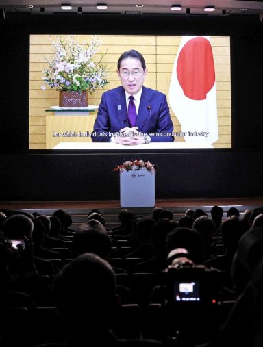
According to Kyodo News on the 24th, TSMC held the opening ceremony at its No. 1 factory in Kumamoto Prefecture, Kyushu, Japan. Attendees included TSMC founder C.C. Chang, Chairman Mark Liu, Japan’s Minister of Economy, Trade and Industry Gen Saito, Kumamoto Governor Ikuo Kabashima, Sony Group Chairman Kenichiro Yoshida, and Toyota Chairman Akio Toyoda. Although Japanese Prime Minister Fumio Kishida did not attend the ceremony, he stated in a video message that "semiconductors are indispensable technology for digitalization and decarbonization."
TSMC’s No. 1 factory in Kumamoto Prefecture is located on approximately 210,000 square meters of land in Kikuyo-machi, a rural village that used to cultivate cabbage and carrots. The site includes a FAB building with cleanrooms, an office building, and gas storage facilities, with the cleanroom area alone covering 45,000 square meters. It is expected that manufacturing equipment will be brought in and installed during the first half of this year, with mass production starting from the fourth quarter.
The factory operation will be managed by a subsidiary established by TSMC for the Kumamoto No. 1 factory called Japan Advanced Semiconductor Manufacturing (JASM). In addition to TSMC as the major shareholder, Japanese companies such as Sony and Denso also participated in JASM’s investment. Sony Group Chairman Yoshida said at the opening ceremony, "We have much to learn from TSMC."
JASM employs about 400 expatriates dispatched from Taiwan, approximately 200 personnel dispatched from Sony Group, and local hires, totaling 1,700 employees. They plan to produce about 55,000 wafers (300mm wafer equivalent) per month using 12 to 28 nanometer (nm, one billionth of a meter) process technology. Currently, the most advanced mass production technology is 3nm, so it is difficult to say that the Kumamoto No. 1 factory has cutting-edge processes. However, the latest mass production process available in the Japanese industry is 40nm, making the Kumamoto No. 1 factory the most advanced semiconductor mass production facility in Japan.
The Japanese government decided to provide subsidies up to 476 billion yen (approximately 4.2 trillion won) to attract TSMC’s factory. This amount is close to half of the investment in the No. 1 factory’s facilities. Besides the TSMC factory, semiconductor factories of related companies such as Sony Group are also gathering, and TSMC announced plans to build a second factory aiming to start operations by the end of 2027. The second factory is planned to produce more advanced products than the first. The Japanese government will also support the second factory with 730 billion yen, meaning government subsidies exceeding 1 trillion yen will be invested.
Founder C.C. Chang evaluated the Kumamoto No. 1 factory at the opening ceremony as "a renaissance of semiconductor production in Japan." Additionally, Minister Saito said about the second factory, "It will greatly contribute to the stable supply of advanced semiconductors."
© The Asia Business Daily(www.asiae.co.kr). All rights reserved.
![Clutching a Stolen Dior Bag, Saying "I Hate Being Poor but Real"... The Grotesque Con of a "Human Knockoff" [Slate]](https://cwcontent.asiae.co.kr/asiaresize/183/2026021902243444107_1771435474.jpg)


