KAIST Research Team Develops Bipolar Multifunctional Electronic Device Based on Molybdenum Disulfide (MoS2)
Expanding Practicality of 2D Semiconductor Materials and Anticipating Future IC Miniaturization
Facilitating Custom Semiconductor Fabrication Composed of Devices with Different Functions
A bipolar multifunctional electronic device that overcomes the drawbacks of molybdenum disulfide (MoS2), which has better performance than conventional silicon semiconductors, has been developed by a domestic research team. It is attracting attention as a potential turning point to continue the miniaturization of semiconductor processes that are reaching their limits.
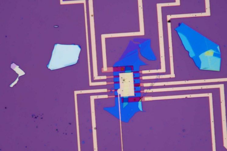 Multifunctional electronic device made of molybdenum disulfide material developed by Professor Gayoung Lee's team at KAIST. Photo by KAIST
The advancement of semiconductors is a competition to reduce circuit line widths. The 'Moore's Law,' which states that semiconductor integration doubles every year, has now reached its limit. Securing fine processes is essential to miniaturize semiconductors and reduce heat generation and power consumption, but concerns are growing that existing silicon materials have clear limitations.
For this reason, two-dimensional semiconductors are emerging as next-generation semiconductor materials. Two-dimensional materials have a thickness of a single atomic layer. Representative examples include graphene and molybdenum disulfide (MoS2). Active research is also being conducted in the industry by companies such as TSMC and Intel.
Among them, molybdenum disulfide has N-type semiconductor characteristics through which electrons flow and is stable in the atmosphere. The problem is that the drawbacks of molybdenum disulfide are critical. It is difficult to implement as a P-type semiconductor. Although methods such as introducing additional processes to molybdenum disulfide or using other P-type materials exist, the high process difficulty has been an obstacle to commercialization.
The multifunctional electronic device based on a two-dimensional nano semiconductor with bipolar semiconductor characteristics developed by Professor Gayoung Lee's research team at the Department of Electrical Engineering at KAIST is expected to be an important breakthrough to overcome the drawbacks of molybdenum disulfide.
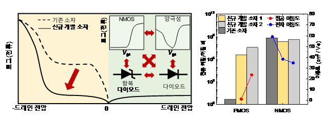 Research Summary and Newly Developed Device with Ambipolar Semiconductor Characteristics Compared to Existing Devices
Professor Lee Gayoung's research team succeeded in implementing bipolar characteristics that allow both electrons and holes to selectively flow by placing electrodes under the channel using single molybdenum disulfide material and improving the metal/semiconductor junction characteristics.
 Professor Gayoung Lee, Department of Electrical Engineering, KAIST
 (From left) Song Jun-gi, Integrated MS-PhD Program, Department of Electrical Engineering, KAIST; Lee Soo-yeon, Master's Program
A multifunctional electronic device is a device that can change its function depending on the voltage, unlike conventional transistors. The team's device can be converted into a bipolar transistor, N-type transistor, diode, avalanche diode, and photodetector, enabling a wide range of applications. Since multiple devices performing various functions can be integrated into one, it is expected to contribute to the miniaturization of integrated circuit (IC) chips.
Students Junki Song and Suyeon Lee, who led this research, said, “We implemented various functions of next-generation two-dimensional semiconductors through a process highly compatible with existing silicon CMOS processes,” adding, “This will be an opportunity to expand the applicability and practicality of molybdenum disulfide electronic devices in IC chips.”
Professor Lee Gayoung introduced, "The device developed this time is differentiated from previous studies in that it was made by a much simpler method than those previously reported." She also explained, "Unlike graphene, it can both turn current on and off, performing various functions according to the given voltage characteristics while maintaining excellent performance for each function." Professor Lee added, “Since multifunctionality is possible in a single device, it is expected to facilitate the production and process transition of customized semiconductors and contribute to the miniaturization of single-chip systems.”
This research, co-first authored by Junki Song, a combined master's and doctoral student, and Suyeon Lee, a master's student in the Department of Electrical Engineering at KAIST, was published online on January 26, 2024, in the prestigious international journal in the field of nanoscience, `ACS Nano' (Paper title: Drain-induced multifunctional ambipolar electronics based on junctionless MoS2).
Meanwhile, this research was conducted with support from the Basic Research Program of the National Research Foundation of Korea, BK21, KAIST's C2 (Creative & Challenging) project, and the LX Semicon-KAIST Future Technology Center.
© The Asia Business Daily(www.asiae.co.kr). All rights reserved.
![Clutching a Stolen Dior Bag, Saying "I Hate Being Poor but Real"... The Grotesque Con of a "Human Knockoff" [Slate]](https://cwcontent.asiae.co.kr/asiaresize/183/2026021902243444107_1771435474.jpg)


