South Korea's semiconductor-related 'Cavity substrate design technology' will be established as an international standard.
The National Institute of Technology and Standards under the Ministry of Trade, Industry and Energy announced that from the 6th to the 10th, the 'International Electrotechnical Commission Technical Committee 91 (IEC/TC91)' general meeting will be held at the Jeju Ocean Suites Hotel, with over 50 standard experts from 9 countries including the United States, Germany, and Japan participating.
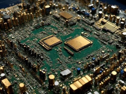
IEC/TC91 is an organization that sets international standards across a wide range of areas including semiconductor chip and component packaging, printed circuit board (PCB) materials, and bonding technologies.
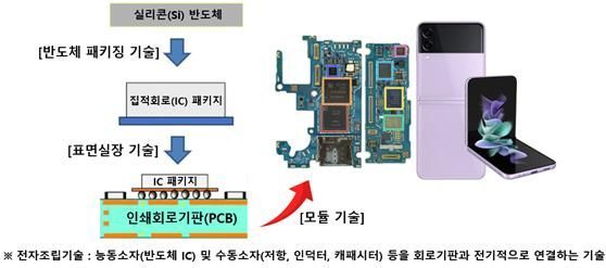
At this meeting, follow-up discussions will be held on the international standard proposal for the 'Cavity (groove for component bonding) substrate design technology' developed by South Korea. This standard proposal involves a technology that forms grooves (cavities) on substrates to miniaturize semiconductor packages and is currently at the final approval stage for international standardization. Once it passes the last procedure and is established as an international standard, it is expected to contribute to the market expansion of Korean companies preparing for commercialization of this technology.
South Korea will also propose a new international standard for 'laser bonding technology' at this meeting. This standard proposal includes criteria for the scanning time and intensity of lasers used to bond electronic components and printed circuit boards. As electronic products become smaller and lighter, the demand for ultra-small semiconductor chips is increasing, and laser bonding technology is evaluated as a technology that can reduce warpage and energy loss by using lasers instead of the traditional method of heating the entire substrate.
The standard proposal will be approved with the support of more than two-thirds of the member countries of the related technical committee, after which discussions on standard development will proceed.
Jin Jong-wook, Director of the National Institute of Technology and Standards, said, "Electronic assembly technology has a wide and diverse range of applications, from personal smartphones in daily life to high-performance artificial intelligence computing equipment," and added, "We will actively support broad international standardization activities to expand the global market for Korean companies."
© The Asia Business Daily(www.asiae.co.kr). All rights reserved.
![Clutching a Stolen Dior Bag, Saying "I Hate Being Poor but Real"... The Grotesque Con of a "Human Knockoff" [Slate]](https://cwcontent.asiae.co.kr/asiaresize/183/2026021902243444107_1771435474.jpg)


