TSMC's 3nm Sales Share at 6%...
Samsung Electronics Cannot Even Disclose Sales Share
Analysis Suggests Comparability Starting from 2nd Generation 3nm Products
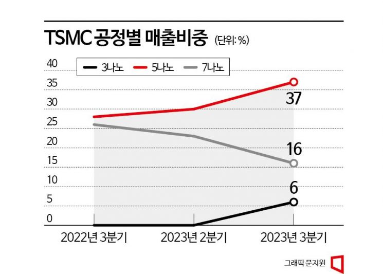
3㎚ (nanometer, one billionth of a meter) 6%, 5㎚ 37%, 7㎚ 16%.
The world’s number one foundry (semiconductor contract manufacturing) company TSMC’s revenue share from advanced processes below 7 nanometers in the third quarter of this year reached 59%. This is not only 6 percentage points higher than the previous quarter, the second quarter of this year, but also 5 percentage points higher compared to 54% in the third quarter of last year. Semiconductor chips express performance by nanometers, which indicate the linewidth of fine circuits, and generally, processes below 7 nanometers are classified as advanced processes. Samsung Electronics and TSMC are currently at the stage of mass-producing semiconductors using 3-nanometer processes, beyond 7-nanometer and 5-nanometer processes.
TSMC disclosed the revenue share of the 3-nanometer process for the first time this year. 6% of the total wafer revenue came from the 3-nanometer process, which began mass production at the end of last year. Considering the total revenue of 546.73 billion US dollars (approximately 22.8 trillion Korean won), this means about 1.36 trillion Korean won came from the 3-nanometer process.
Samsung Electronics, which started mass production of the world’s first 3-nanometer first-generation process six months earlier than TSMC, is unlikely to disclose the revenue share of the 3-nanometer process when announcing its confirmed third-quarter results on the 31st. Samsung Electronics only discloses the revenue and operating profit of its semiconductor division (DS) in its overall performance, but does not separately classify and disclose foundry performance, which is a non-memory area. Unlike TSMC, it also does not reveal the revenue share by advanced process or by platform such as HPC, smartphones, or automobiles.
The semiconductor industry views that although TSMC’s 3-nanometer process revenue share is lower than expected, it would have been impossible for Samsung Electronics to have earned more revenue from the 3-nanometer process than TSMC. In other words, TSMC’s world-first disclosure of the 3-nanometer revenue share can be interpreted as confidence in market preemption.
Samsung Electronics mass-produced the world’s first 3-nanometer semiconductor in June last year. It also applied Gate-All-Around (GAA) technology, which will be used in TSMC’s 2-nanometer process mass production in 2025, first. GAA is a structure that increases the contact surface between the transistor gate (the door through which current flows) and the channel (the path where current flows) to four sides, offering higher power efficiency than the existing FinFET technology, solving issues such as current leakage and heat generation.
Nevertheless, major semiconductor customers chose TSMC over Samsung Electronics as the foundry to produce 3-nanometer chips first. Apple equipped the premium iPhone 15 Pro among the new iPhone 15 series with the A17 Pro chip made by TSMC’s 3-nanometer process. Since Apple competes with Samsung Electronics in smartphones, it is not easy for Apple to entrust Samsung Electronics with production orders for core semiconductors to be installed in the latest smartphones.
For Samsung Electronics to catch up with TSMC, which has long experience and trust in the foundry sector, it must gain recognition for its GAA technology in processes below 3 nanometers and stably secure global major customers. According to market research firm TrendForce’s data as of the first half of this year, Samsung Electronics and TSMC’s foundry market shares are 11.7% and 56.4%, respectively, a gap of 44.7 percentage points. Compared to the record at the end of last year?Samsung Electronics 15.8%, TSMC 58.5%?the market share gap has widened.
However, some analysts suggest that Samsung Electronics may not be overly concerned about TSMC’s 3-nanometer revenue share figure of 6%. Since Samsung introduced GAA technology earlier than TSMC and is working on yield stabilization, the number can be overturned once foundry demand recovers. The industry estimates Samsung Electronics’ GAA-based 3-nanometer semiconductor yield to be over 60%. On the other hand, TSMC started adopting GAA technology three years later than Samsung Electronics, so it may experience trial-and-error with low yields in the early stages of mass production. From Samsung Electronics’ perspective, unlike the 3-nanometer first-generation process, which struggled to secure customers, the 3-nanometer second-generation process to be mass-produced next year presents an opportunity to stand out in market preemption over TSMC’s 3-nanometer semiconductors.
© The Asia Business Daily(www.asiae.co.kr). All rights reserved.
![Clutching a Stolen Dior Bag, Saying "I Hate Being Poor but Real"... The Grotesque Con of a "Human Knockoff" [Slate]](https://cwcontent.asiae.co.kr/asiaresize/183/2026021902243444107_1771435474.jpg)


