Applied Materials Unveils New Equipment
Energy Consumption Reduced by 35% Compared to Previous Generation
"Commercialization Expected Starting from Memory Semiconductor Industry"
"The cost of semiconductor manufacturing is increasing, and the required performance is also rising. By utilizing the Vistara platform, we can accelerate the speed from semiconductor chip development to mass production while maximizing productivity and yield (the ratio of good products among finished products)."
Jang Daehyun, Head of Memory Etch Technology at Applied Materials Korea, said this at a press briefing held on the 30th at the company's headquarters office in Bundang-gu, Seongnam-si. He explained that the company developed equipment that processes multiple steps in a vacuum state in one place after more than four years of development, and that it will first be introduced in the memory semiconductor field.
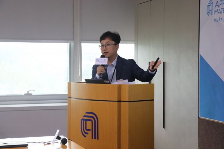 Jang Daehyun, Head of Memory Etch Technology at Applied Materials Korea, is giving a presentation at the headquarters office in Bundang, Seongnam City on the 30th. / [Photo by Applied Materials Korea]
Vistara is the fifth equipment platform introduced by Applied Materials for wafer production. The company launched Endura in 1990, Centura in 1992, Producer in 1998, and Centris in 2010, and released a new equipment platform after 13 years. This product focuses on solving the increasing challenges that come with semiconductor technology advancement.
Jang said, "The cost per unit area of (wafer) output is gradually increasing, product complexity is rising, and the time required for production is also increasing," adding, "Carbon emissions are also increasing due to higher energy consumption." He further explained that "Vistara was developed based on three pillars: flexibility, intelligence, and sustainability" to address these issues.
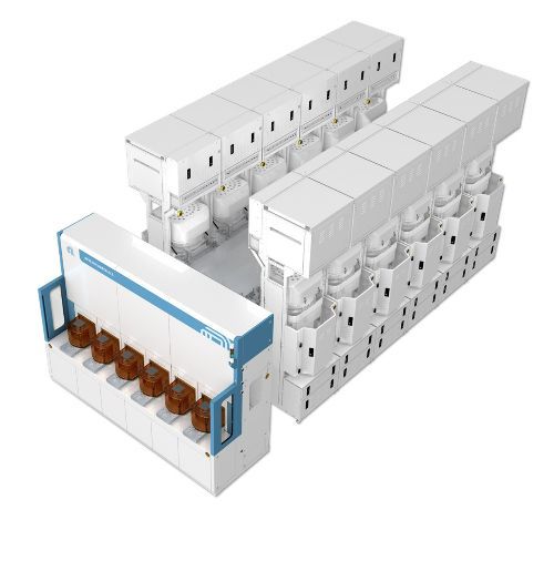 Image of the Vistara platform introduced by Applied Materials /
 [Image provided by Applied Materials Korea]
Vistara can be equipped with up to 12 process chambers. The size and structure of the chambers can also be selected in various ways. The chambers are vacuum spaces where various chemical reactions and processes occur during semiconductor chip manufacturing. By conducting multiple processes on one platform through multiple chambers, technological precision can be enhanced.
Through thousands of sensors and supporting software installed in Vistara, real-time data is analyzed by artificial intelligence (AI) to reduce errors and defects that may occur during mass production. This means that product launch time can be shortened, and productivity and yield can be increased. Compared to previous generation equipment, energy consumption can also be reduced by up to 35%.
The equipment will be used in the memory, logic (system), and foundry (semiconductor contract manufacturing) sectors. Currently, major customers in these fields are preparing to apply Vistara. The memory industry will be the first to utilize it. The company explained that "it will be used to reduce the recently increasing etching process time" and "commercialization will be possible soon."
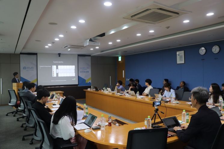 An office of Applied Materials Korea located in Bundang, Seongnam City, where a press conference is being held /
 [Photo by Applied Materials Korea]
Meanwhile, Applied Materials expects the importance of heterogeneous integration packaging technology, which combines different semiconductor chips to maximize performance, to increase in the future. This is the background for unveiling new hybrid bonding and through-silicon via (TSV) technologies used in packaging last month. The company is currently discussing technology and applications with various customers. It is also known to be collaborating with Samsung Electronics and SK Hynix, who are launching high-bandwidth memory (HBM) for AI using related technologies.
Park Heungrak, Head of Packaging Technology at Applied Materials Korea, said, "The company has held an important position in the front-end (the process of manufacturing semiconductor chips from wafers) equipment sector," adding, "As the packaging field develops in the future, we aim to strengthen our capabilities in this area as well."
© The Asia Business Daily(www.asiae.co.kr). All rights reserved.
![Clutching a Stolen Dior Bag, Saying "I Hate Being Poor but Real"... The Grotesque Con of a "Human Knockoff" [Slate]](https://cwcontent.asiae.co.kr/asiaresize/183/2026021902243444107_1771435474.jpg)


