KAIST Develops Heat Transfer Method Using Surface Waves on Metal Thin Films
Transfers Heat 25% Better Than Existing Methods
Solves Heat Generation Issues from Semiconductor Device Miniaturization
Domestic researchers have developed a new technology that can solve the heat generation phenomenon caused by high integration of semiconductors.
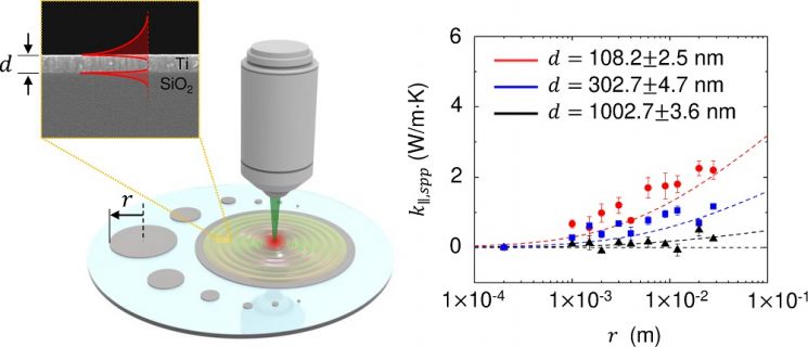
KAIST announced that a research team led by Professor Bong-Jae Lee from the Department of Mechanical Engineering has succeeded for the first time in the world in measuring a new heat transfer mode generated by 'surface plasmon polaritons' in metal thin films deposited on substrates. Surface plasmon polaritons refer to surface waves formed on metal surfaces as a result of strong interactions between electromagnetic fields at the dielectric-metal interface and free electrons on the metal surface, which collectively oscillate as quasiparticles.
Recently, due to the miniaturization of semiconductor devices, heat generated at hot spots is not effectively dispersed, leading to reduced reliability and durability of the devices. Existing thermal management technologies have limitations in managing the increasingly severe heat generation issues. As devices become more integrated, an approach based on a fundamental understanding of heat transfer phenomena at extreme scales, beyond traditional thermal management technologies, is required.
The research team discovered a new heat transfer method caused by surface waves generated in metal thin films deposited on substrates and proposed a solution. To improve heat diffusion in metal thin films with nanoscale thickness, they utilized surface plasmon polaritons, which are surface waves occurring at the metal-dielectric interface. This new heat transfer mode occurs when metal thin films are deposited on substrates, making it highly applicable in device fabrication processes and allowing production over large areas. The team demonstrated that the thermal conductivity increased by about 25% due to surface waves generated in a titanium thin film approximately 100 nanometers thick with a radius of about 3 cm.
Professor Lee said, "The significance of this research lies in being the first in the world to identify a new heat transfer mode caused by surface waves occurring in metal thin films deposited on substrates with low process difficulty," adding, "It can be applied as a nanoscale heat spreader that effectively disperses heat near hot spots inside ultra-high heat semiconductor devices."
The research team's findings have significant implications for the future development of high-performance semiconductor devices, as they can be applied to rapidly disperse heat in the planar direction in nanoscale thickness thin films. In particular, while thermal conductivity decreases in nanoscale thickness thin films due to boundary scattering, this newly identified heat transfer mode enables effective heat transfer even at nanoscale thicknesses, which is expected to fundamentally solve the unit thermal management issues of semiconductor devices.
This research was published online on the 26th of last month in the international academic journal Physical Review Letters.
© The Asia Business Daily(www.asiae.co.kr). All rights reserved.
![Clutching a Stolen Dior Bag, Saying "I Hate Being Poor but Real"... The Grotesque Con of a "Human Knockoff" [Slate]](https://cwcontent.asiae.co.kr/asiaresize/183/2026021902243444107_1771435474.jpg)


