Professor Kim Jungwon's KAIST Research Team
Develops 'Ultrafast Camera' for Real-Time Imaging of Internal Dynamics
South Korea's Samsung Electronics and Taiwan's TSMC are fiercely competing to secure yield rates for 3-nanometer semiconductors, and meanwhile, South Korean scientists have developed a technology that can dramatically improve semiconductor yield. This technology enables real-time ultra-high-speed, high-resolution imaging inside semiconductor devices to identify and correct issues. It is drawing attention as a potential 'game changer' that could determine the outcome of the semiconductor war between Korea and Taiwan.
On the 26th, the National Research Foundation of Korea announced that a research team led by Professor Kim Jeong-won at the Korea Advanced Institute of Science and Technology (KAIST) developed an ultra-high-speed camera technology capable of measuring the fine structures and dynamic characteristics inside semiconductor devices with high resolution.

As the development of micro- and nano-devices with increased complexity and functionality has been rising recently, the need for technology that can measure fine structures and movements inside devices in real time has grown. The semiconductor industry, with the advancement of various three-dimensional integrated circuits and devices, demands fine structure measurement technologies that offer higher resolution and faster measurement speeds over larger wafer areas. Measuring dynamic characteristics is fundamental for understanding various physical phenomena within devices and developing applied technologies, thus requiring higher resolution, faster measurement speeds, and larger measurement ranges. Existing measurement technologies have limitations in achieving such complex performance.
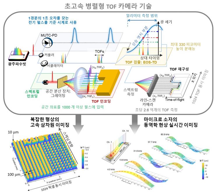
The research team developed an ultra-high-speed camera technology capable of precisely and accurately measuring complex three-dimensional shapes at high speed, successfully observing complex and irregular high-speed dynamic phenomena. They split light pulses with a pulse width of 100 femtoseconds (one ten-trillionth of a second) into more than 1,000 colors, then used pulses of different colors to precisely measure height variations at different spatial locations. This technology is so fast and precise that it can measure height differences of 260 million pixels per second down to the level of 330 picometers (one three-billionth of a meter). The ultra-high-speed camera technology, with its high-speed shape imaging and high spatial resolution, can monitor and control semiconductor processes and 3D printing processes, which are becoming increasingly advanced and integrated, in real time, thus expected to significantly contribute to improving process yield.
The research team measured height variations of two-dimensional surfaces by scanning a one-dimensional line-shaped light beam in a moving manner, but plans to develop the technology further to measure height variations of two-dimensional surfaces all at once without scanning.
Professor Kim explained, “The new ultra-high-speed camera technology can capture movements of fine structures that have various amplitudes and simultaneously very fast instantaneous speeds,” adding, “It will evolve into next-generation measurement technology to explore complex physical phenomena that have not been observed before.”
The research results were published on the 15th in the international optical journal Light: Science & Applications.
© The Asia Business Daily(www.asiae.co.kr). All rights reserved.
![Clutching a Stolen Dior Bag, Saying "I Hate Being Poor but Real"... The Grotesque Con of a "Human Knockoff" [Slate]](https://cwcontent.asiae.co.kr/asiaresize/183/2026021902243444107_1771435474.jpg)


