Collaboration on GaN Power Semiconductor Foundry Process Technology Development by 2024
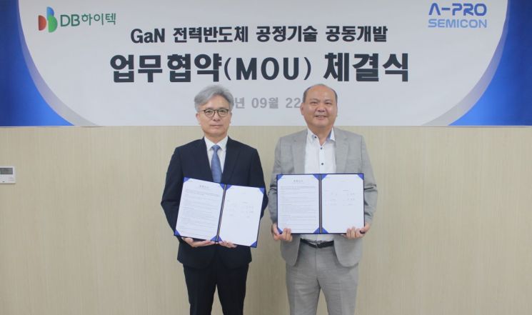 Lim Jong-hyun, CEO of AProsemicon (left), and Cho Ki-seok, Head of Foundry Sales Division at DB HiTek, are taking a commemorative photo after signing a business agreement for the development of GaN power semiconductor foundry process technology. / Source=DB HiTek
[Asia Economy Reporter Kim Pyeonghwa] DB HiTek announced on the 22nd that it has signed a memorandum of understanding (MOU) with the domestic fabless semiconductor design company AProsemicon to collaborate on gallium nitride (GaN) power semiconductors.
The two companies will cooperate from this year through 2024 to develop foundry process technology for GaN power semiconductors. They will jointly develop and secure core processes for GaN power semiconductor products, and each will utilize the acquired technology in their respective businesses. DB HiTek plans to establish a comprehensive partnership, including the application of 8-inch GaN epi wafer products manufactured by AProsemicon.
DB HiTek has selected compound semiconductor businesses such as GaN and silicon carbide (SiC) as next-generation growth engines to expand its foundry business and is conducting research and development (R&D). The technical collaboration with a GaN-specialized fabless company is evaluated as an opportunity to quickly enter the next-generation power semiconductor market. It is also expected to enable stable revenue generation through securing demand sources.
Based on this agreement, AProsemicon has secured a stable foundry partner and can expand its GaN power semiconductor business. The 8-inch GaN power semiconductor technology developed by the two companies is compatible with the 8-inch process equipment owned by DB HiTek, which can lead to stable foundry production. Through cooperation with DB HiTek, AProsemicon’s technological capabilities related to in-house device development have been recognized.
During the cooperation period, DB HiTek plans to purchase and use AProsemicon’s GaN epi wafers. GaN epi wafers are key materials with a high dependence on overseas imports. AProsemicon introduced the first domestic 8-inch MOCVD mass production equipment for GaN power semiconductors in 2020 to produce wafers directly and has started production. Through this agreement, not only will the localization of 8-inch GaN epi wafers be achieved, but sales performance is also expected to follow.
A DB HiTek official said, "Through this technical cooperation with AProsemicon, we have secured future growth engines and laid the foundation to lead the rapidly growing next-generation high value-added power semiconductor market." They explained that forming a value chain connecting materials (AProsemicon), components (DB HiTek), and equipment (APro) is expected to generate additional synergies such as localization and internalization of key core technologies.
The GaN market is projected to grow rapidly at an average annual rate of 49%, from $270 million this year to $2 billion by 2027. Demand is expected to surge in smartphones, various IT devices’ fast charging, and data centers.
© The Asia Business Daily(www.asiae.co.kr). All rights reserved.
![Clutching a Stolen Dior Bag, Saying "I Hate Being Poor but Real"... The Grotesque Con of a "Human Knockoff" [Slate]](https://cwcontent.asiae.co.kr/asiaresize/183/2026021902243444107_1771435474.jpg)

