Attendance at the Groundbreaking Ceremony of the Next-Generation Semiconductor R&D Complex
[Asia Economy Reporter Park Sun-mi] "Let's continue the tradition of prioritizing technology and pioneering investment."
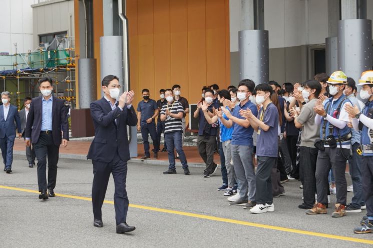
Samsung Electronics Vice Chairman Lee Jae-yong once again emphasized technology on the 19th at the groundbreaking ceremony for the next-generation semiconductor research and development (R&D) complex held at Samsung Electronics Giheung Campus in Yongin, Gyeonggi Province.
Vice Chairman Lee said, "We are starting a new challenge at the Giheung site where the first shovel was dug 40 years ago to build a semiconductor factory," adding, "Without bold R&D investments not only in the next generation but also in the generation after next products, today's Samsung Semiconductor would not exist." He further stated, "Let's continue the tradition of prioritizing technology and pioneering investment," and "Let's create the future with technologies that do not exist in the world."
Recalling the words of the late Chairman Lee Byung-chul that the semiconductor industry is not only highly marketable but also a high value-added industry with significant ripple effects on other industries, he urged securing 'super-gap' technological capabilities that can lead the global market without being shaken by crises.
Samsung Electronics declared at the ceremony, with the slogan "Creating the future with technologies that do not exist in the world," that it will lead innovation based on technological leadership and achieve another great leap forward in the semiconductor business.
About 100 executives and employees attended the event, including Vice Chairman Lee, Kyung Kye-hyun, head of the DS Division, Jung Eun-seung, CTO of the DS Division, Jin Gyo-young, head of Samsung Advanced Institute of Technology, Lee Jung-bae, head of the Memory Business Division,
Choi Si-young, head of the Foundry Business Division, and Park Yong-in, head of the System LSI Business Division.
The Giheung Campus is where Samsung's semiconductor business was born in 1983, and it laid the foundation for the 'semiconductor super-gap' with achievements such as ▲developing the world's first 64M DRAM in 1992 ▲achieving first place in the DRAM market in 1992,
and ▲achieving first place in the memory semiconductor sector in 1993.
The Giheung semiconductor R&D complex will be constructed on approximately 109,000㎡ (about 33,000 pyeong), and Samsung Electronics plans to invest about 20 trillion won by 2028 in developing the research complex, including a semiconductor R&D dedicated line scheduled to start operation in mid-2025.
© The Asia Business Daily(www.asiae.co.kr). All rights reserved.
![Clutching a Stolen Dior Bag, Saying "I Hate Being Poor but Real"... The Grotesque Con of a "Human Knockoff" [Slate]](https://cwcontent.asiae.co.kr/asiaresize/183/2026021902243444107_1771435474.jpg)


