Increasing Yield and Securing Major Customers Are Key in Cutting-Edge Processes Below 3nm
[Asia Economy Reporter Park Sun-mi] Samsung Electronics' decision to hold a product shipment ceremony just one month after announcing the mass production of the world's first 3-nanometer foundry process applying Gate-All-Around (GAA) technology is interpreted as a display of confidence in its superiority over Taiwan's TSMC in advanced processes and a determination to secure 'big-name' customers. Samsung plans to expand production of 3-nanometer products, currently produced only at its Hwaseong campus, to the Pyeongtaek campus as additional 3-nanometer foundry customers are secured.
According to the semiconductor industry on the 25th, it is widely believed that until Samsung Electronics can stably secure global 'big-name' customers such as Apple, Qualcomm, and Intel in the sub-3-nanometer advanced process, it will be difficult to significantly narrow the market share gap with TSMC, the number one foundry in the industry.
Taiwanese market research firm TrendForce analyzed the foundry (semiconductor contract manufacturing) market share for the first quarter of this year as TSMC 53.6% and Samsung 16.3%. Compared to the fourth quarter of last year, TSMC's market share increased by 1.5 percentage points, while Samsung's declined by 2 percentage points, widening the gap to 37.3 percentage points.
 On the 25th, at the Samsung Electronics Hwaseong Campus in Hwaseong City, Gyeonggi Province, the world's first mass shipment ceremony for 3nm production based on GAA was held. The 3nm process is the most advanced technology in semiconductor manufacturing processes, and GAA is also known as a next-generation core technology that enhances semiconductor efficiency through precise control. / Hwaseong - Photo by Kim Hyunmin kimhyun81@
The key to changing the atmosphere lies in how many big-name customers Samsung Electronics can secure in the sub-3-nanometer advanced process. Foundry processes are becoming increasingly miniaturized and the difficulty is rapidly rising. Samsung's application of GAA technology for the first time in the industry in this 3-nanometer process once again proves its 'innovative technological capability.' Previously, Samsung introduced EUV equipment to system semiconductors (7-nanometer, 2019) and memory (3rd generation 10-nanometer-class DRAM, 2020), demonstrating overwhelming technological competitiveness.
GAA refers to a technology where the gate surrounds the entire channel, including the bottom surface through which current flows, allowing for more precise control of current flow compared to the existing 3D structure of FinFET. The industry expects TSMC to challenge 3-nanometer foundry mass production as early as the third quarter, but this will likely apply the existing FinFET structure rather than GAA technology. The prevailing view is that TSMC will be able to apply GAA technology starting with the 2-nanometer process in 2025.
Even if Samsung Electronics and TSMC both succeed in mass-producing 2-nanometer foundry processes in 2025, it is possible to analyze that TSMC may lag behind Samsung in terms of technological capability because Samsung applied GAA technology three years earlier, enhancing stability. For example, Samsung's 1st generation 3-nanometer GAA process reduces power consumption by 45% and improves performance by 23% compared to the existing 5-nanometer FinFET process. The size is reduced by 16%. This means that more functions and higher performance can be integrated into semiconductors through ultra-fine processes with GAA applied.
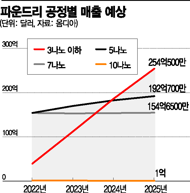
Especially in the foundry process below 10 nanometers, where only Samsung and TSMC compete, the 10-nanometer segment is expected to have an average annual growth rate of -9.4% until 2025, whereas the sub-3-nanometer fine process is forecasted to grow rapidly at 85.6%.
A semiconductor industry insider said, "TSMC, with its long foundry experience, holds a much higher overall market share because it has secured more share in processes that do not require much technological capability compared to Samsung," adding, "Samsung is focusing on ultra-fine processes with high growth potential based on advanced technology, so it now faces an opportunity to gain an advantage in the competition below 3 nanometers." He continued, "It will not be easy for customers to exclude Samsung, which can secure high yields (good product ratios) through earlier mass production," and predicted, "Since Samsung is ahead in production timing, improving yields is only a matter of time."
Meanwhile, Samsung Electronics aims to secure more than 300 customers by 2026, leveraging advanced technologies such as 3-nanometer and 2-nanometer processes.
© The Asia Business Daily(www.asiae.co.kr). All rights reserved.
![Clutching a Stolen Dior Bag, Saying "I Hate Being Poor but Real"... The Grotesque Con of a "Human Knockoff" [Slate]](https://cwcontent.asiae.co.kr/asiaresize/183/2026021902243444107_1771435474.jpg)


