Government Announces Semiconductor Support Measures... Regulatory and Permit Exceptions Expected
Special Floor Area Ratio Exceptions for Semiconductor Complexes... Increased Up to 490%
Mandatory Fast-Track Permit Processing... Amendment of Advanced Strategic Industry Act Planned
Special Extended Working Hours System Expanded to Semiconductor R&D... 64-Hour Workweek
Self-Reliance Rate of SoBuJang Raised from 30% to 50%... 300 Billion Won Fund Also Established
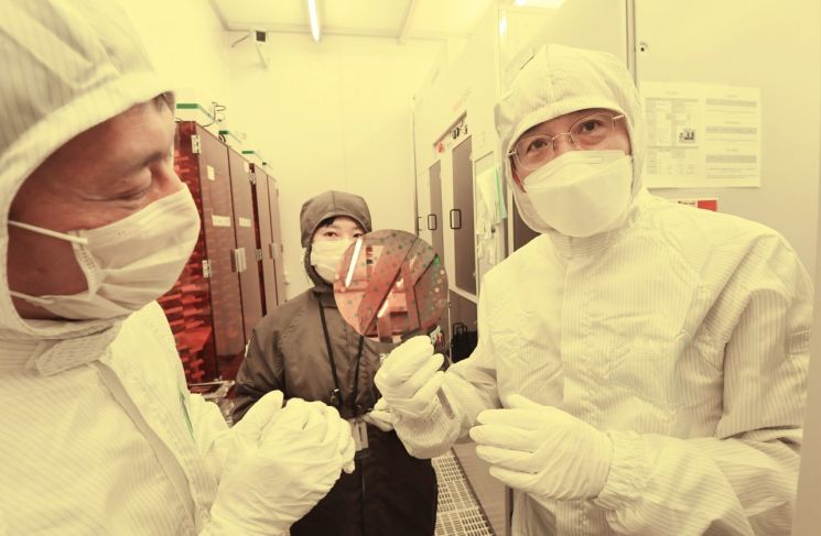 Deputy Prime Minister Choo Kyung-ho Visits Seoul National University Semiconductor Joint Research Center
(Seoul=Yonhap News) Deputy Prime Minister and Minister of Economy and Finance Choo Kyung-ho (right) visited the Semiconductor Joint Research Center at Seoul National University Gwanak Campus on May 31, 2022, touring the facilities. 2022.5.31 [Provided by the Ministry of Economy and Finance. Resale and DB reproduction prohibited]
photo@yna.co.kr
(End)
<Copyright(c) Yonhap News Agency, Unauthorized reproduction and redistribution prohibited>
[Asia Economy Sejong=Reporter Lee Jun-hyung] The government’s “Strategy to Achieve Semiconductor Superpower Status” announced on the 21st is an expression of its determination to not fall behind but take the lead in the increasingly fierce global technological hegemony competition. Governments including the United States, China, and the European Union (EU) have already designated semiconductors as a core item of economic security and are making all-out efforts to support large-scale investments. In fact, the U.S. is discussing a bill to support $52 billion (about 68 trillion KRW) in investment over five years for related facilities and research and development (R&D) to foster its domestic semiconductor industry. Japan urgently allocated a large-scale subsidy of 774 billion yen (7.4 trillion KRW) through a supplementary budget last year to actively support semiconductor companies.
The competition to attract global semiconductor companies is also fierce. Japan supported TSMC, the foundry (contract manufacturing) leader, with about 4.5 trillion KRW for the factory it built in Kumamoto Prefecture. This amount corresponds to about 40% of the investment cost (about 11 trillion KRW) TSMC spent to build the factory. Germany provided about 8.9 trillion KRW, which is 40% of the total investment cost (22 trillion KRW), to Intel’s Magdeburg factory. A government official explained, “Compared to the large-scale investment incentives of competing countries, domestic subsidies and tax support are relatively insufficient,” adding, “The cost advantage of domestic semiconductor production may be reversed.”
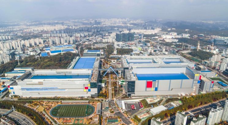 Samsung Electronics Begins World’s First Mass Production of 3-Nanometer Semiconductors...Breaking the Limits of Fine Process Technology
(Seoul=Yonhap News) Samsung Electronics officially announced on the 30th of last month that it has started the initial mass production of 3-nanometer (nm) process foundry (semiconductor contract manufacturing) for the first time in the world.
This 3-nanometer process is produced at Samsung Electronics’ Hwaseong Campus S3 line, where advanced foundry EUV (extreme ultraviolet) process technology is applied. The photo shows the view of Samsung Electronics Hwaseong Campus. 2022.6.30 [Provided by Samsung Electronics. Redistribution and DB reproduction prohibited]
Photo by Samsung Electronics
(End)
<Copyright(c) Yonhap News Agency, Unauthorized reproduction and redistribution prohibited>
Floor Area Ratio Increased by 1.4 Times
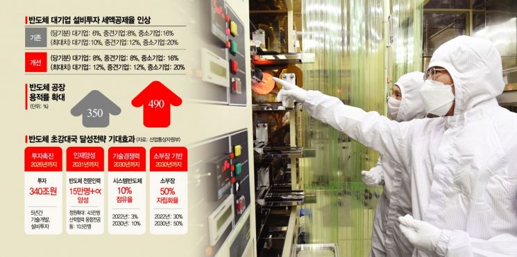
This is why the government announced large-scale regulatory and permit exceptions for semiconductor companies in the strategy released that day. A representative example is applying floor area ratio exceptions to key domestic semiconductor industrial complexes. The government plans to revise the Enforcement Decree of the National Land Planning Act in December to raise the floor area ratio for large-scale semiconductor complexes from the current 350% to up to 490%. The idea is to maximize the allowable capacity for new and expanded semiconductor facilities on limited land by increasing the floor area ratio.
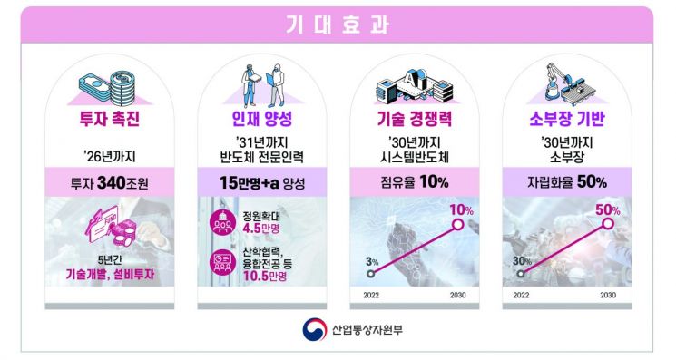
The expected effect is considerable. If the floor area ratio increases as planned by the government, the number of clean rooms at Samsung Electronics’ Pyeongtaek campus will increase from 12 to 18. The clean rooms in the semiconductor cluster that SK Hynix is building in Yongin, Gyeonggi Province, will expand from 9 to 12. Considering that each clean room generates employment for about 1,000 people, this means a total employment increase of 9,000 people.
Measures to expedite permits for semiconductor complexes will also be promoted. This is in consideration of the fact that the construction of SK Hynix’s Yongin semiconductor cluster has been delayed for years due to permit delays. Accordingly, the government plans to revise the “Special Act on National Advanced Strategic Industries,” which is scheduled to be enforced next month, to strengthen special provisions for expedited permit processing for semiconductor complexes. Upon revision of the law, local governments will be required to promptly process permits related to semiconductor complex development unless there are serious or obvious reasons not to do so.
Expansion of Special Extended Working Hours System
Labor and safety regulations will also be relaxed. The government will first recognize exceptions to statutory working hours for the semiconductor industry starting in September. The scope of the special extended working hours system, which was limited to R&D for items subject to Japan’s export restrictions, will be expanded to cover R&D across all semiconductor fields. Under the special extended working hours system, working hours capped at 52 hours per week can be extended up to 64 hours. An official from the Ministry of Trade, Industry and Energy said, “We considered the semiconductor industry’s characteristic of requiring intensive short-term R&D,” adding, “We plan to revise the special extended working hours work guidelines by September.”
The “Semiconductor Academy,” which will serve as a control tower for workforce training, will be established within this year. The Semiconductor Association will be responsible for the curriculum, and companies will support instructors and equipment. The government will provide national funding for operating expenses from next year through 2027. The government plans to operate education programs based on industry demand in stages and train more than 3,600 field personnel over the next five years.
Incentives for outstanding overseas talent have also been prepared. The government is promoting a plan to extend the income tax reduction period from the current five years to ten years for foreign technicians who get employed by domestic companies or research institutes. The same income tax reduction benefits will apply to outstanding domestic personnel who have worked for more than five years at overseas research institutions and then get employed by domestic companies.
Targeting 50% Self-Reliance Rate for Materials, Parts, and Equipment
The self-reliance rate for materials, parts, and equipment (MPE), which supports the semiconductor industry, will be raised to 50% by 2030. The MPE self-reliance rate is about 30% as of this year. The direction of MPE R&D will shift from the existing “catch-up type localization” to “market-leading type.” This is to preemptively respond to changes in the global supply chain and secure the future MPE market. To this end, the proportion of leading technology development in MPE R&D projects will be more than doubled from 9% this year to 20% next year.
Financial support for MPE will also be strengthened. The government will establish a 300 billion KRW fund next year through a public-private partnership to support investment and mergers and acquisitions (M&A) of MPE companies. Semiconductor companies and policy finance will provide 150 billion KRW, and the remaining half will be raised by private financial institutions. The government will also consider preparing a 250 billion KRW “Special Finance for Large and Small-Medium Cooperation in MPE” to provide interest loss compensation for facility investments in core strategic MPE items.
Minister of Trade, Industry and Energy Lee Chang-yang said, “We will sequentially establish plans to strengthen the competitiveness of industries that will drive future demand for semiconductors, such as batteries and displays,” adding, “We will continue to promote educational innovation and industry cooperation to nurture not only semiconductor but also software (SW) personnel.”
© The Asia Business Daily(www.asiae.co.kr). All rights reserved.


