Series of internationally recognized research results including next-generation high-density semiconductor technology
 Next-generation automotive system semiconductor by Samsung Electronics. Stock photo. Not related to the article.
[Asia Economy Reporter Kim Bong-su] Amid fierce competition in high-density semiconductor technology between Samsung Electronics and Taiwan's TSMC, a next-generation technology that can accelerate the realization of a 'super-gap' semiconductor powerhouse in Korea has been developed.
On the 2nd, Professor Shin Hyun-seok's research team at Ulsan National Institute of Science and Technology (UNIST) devised a core technology for developing next-generation high-density semiconductors capable of breaking 'Moore's Law,' which was published in the prestigious international journal Nature. Moore's Law, established by Intel's Gordon Moore, means that the density of transistors (microdevices) integrated into semiconductor integrated circuits (IC chips) doubles every two years.
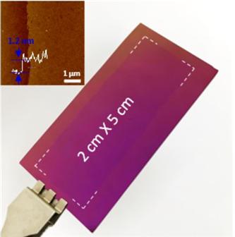
The research team overcame this limitation by developing the world's first technology to synthesize hexagonal boron nitride (hBN) single crystals in multiple layers. Hexagonal boron nitride is known as the only two-dimensional insulating material that can prevent functional degradation such as charge traps and charge scattering that may occur in next-generation high-density semiconductors. However, developing technology to synthesize it in a single-crystal form with an appropriate thickness suitable for semiconductor devices was a challenge. By controlling the concentration of materials required for synthesis through a new synthesis method, the research team synthesized thickness-controllable hexagonal boron nitride single crystals for the first time in the world.
Professor Shin explained, "We have developed a material synthesis technology that can overcome the physical limitations of existing high-density semiconductors," adding, "Hexagonal boron nitride can be used not only for semiconductors but also for hydrogen fuel cell electrolyte membranes, next-generation secondary battery electrode materials, quantum light sources, and more, so active additional research is needed to secure foundational technology for material production."
Professor Kim Yoon-seok's research team at Sungkyunkwan University recently devised a world-first method to dramatically enhance the ferroelectricity of hafnium oxide (HfO2), a next-generation semiconductor material. Additionally, on the 27th of last month, the research team led by Professors Jeon Seok-woo and Shin Jong-hwa at KAIST developed a three-dimensional lithography process, a core technology for next-generation semiconductor processes. This new technology allows lithography to be performed all at once instead of layer by layer, significantly reducing costs and time compared to previous methods.
© The Asia Business Daily(www.asiae.co.kr). All rights reserved.


![The Special Connection Between the Statue of Martyr Lee Jun in Jangchungdan Park and Mayor Oh Sehoon ③ [Current Affairs Show]](https://cwcontent.asiae.co.kr/asiaresize/319/2026012110001599450_1768957215.jpg)