Samsung Unveils Next-Gen 3nm Wafers During Biden's Visit
Mass Production Planned for H1 This Year... A Strategic Move to Narrow Gap with TSMC
Latest 'GAA' Technology Applied, Outperforms TSMC's 'FinFET'
Increased Process Complexity Raises Concerns... Yield May Decline

[Asia Economy Reporter Lim Juhyung, Intern Reporter Song Hyundo] Attention is focused on the semiconductor wafer signed side by side by U.S. President Joe Biden and President Yoon Suk-yeol during Biden's visit to Korea on the 20th. It is Samsung Electronics' world's first 3-nanometer (nm) wafer scheduled for mass production within this year. The 3nm wafer, unveiled to the public for the first time that day, is Samsung's 'secret weapon' developed to catch up with Taiwan's TSMC, the No. 1 foundry in the industry. Not only is it the world's first mass-produced 3nm semiconductor, but it also adopts the 'Gate-All-Around (GAA)' process, which is far more advanced than TSMC's technology.
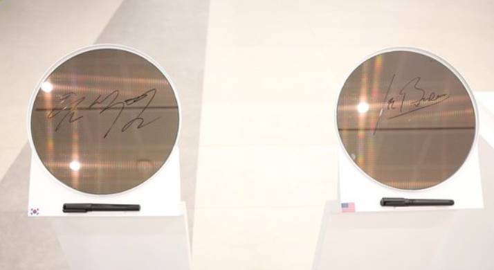 President Joe Biden of the United States and President Yoon Suk-yeol signing Samsung Electronics' next-generation 3-nanometer (nm) wafer. / Photo by Yonhap News
◆Next-generation 3nm wafer unveiled during U.S. President Biden's visit to Korea
President Biden visited Samsung's semiconductor production base in Pyeongtaek, Gyeonggi Province, together with President Yoon on the 20th. At this event, Samsung unveiled its GAA-based 3nm semiconductor wafer to President Biden, and the two presidents of Korea and the U.S. held a surprise event signing the wafer, emphasizing the importance of the Korea-U.S. technological alliance. After touring the 'Line 3' of the Pyeongtaek semiconductor plant, President Biden expressed admiration, saying, "Many technological innovations led by Samsung are astonishing."
Samsung aims to apply 3nm mass production within the first half of this year. If Samsung delivers 3nm semiconductors within the first half, it will claim the title of 'world's first mass production of 3nm' by surpassing TSMC, the No. 1 foundry, which targets the second half of the year.
In fact, Samsung is currently at a disadvantage compared to TSMC in the foundry market. According to market research firm TrendForce, TSMC holds the No. 1 global foundry market share this year, rising 3 percentage points (p) from last year to 56%. Meanwhile, Samsung's share is expected to drop 2%p from last year's 18% to 16%.
Major customers have also left Samsung. Nvidia, the world's largest graphics processing unit (GPU) design company and a Samsung partner, and Qualcomm, famous for smartphone application processors (AP) and communication chip design, each decided last year and in February, respectively, to entrust their processor foundry production to TSMC instead of Samsung.
◆TSMC developed 'GAA' to catch up with 'FinFET'... Will it narrow the technology gap?
Samsung's ace card prepared to overcome this slump and overtake TSMC is GAA technology. GAA is one of the transistor structures used in semiconductors.
Semiconductors are made by integrating transistors that control current flow in circuits. When voltage is applied to the 'gate' part of the transistor, current flows through the passage called the 'channel,' enabling the semiconductor to operate.
As the competition for semiconductor miniaturization intensified, circuit linewidths shrank to the nm scale. Therefore, transistors also had to become smaller. The problem is that as transistors shrink, the gate also miniaturizes, reducing the contact area with the channel. This causes the gate to malfunction and generate leakage current, damaging the transistor.
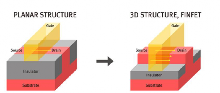 The conventional transistor (left) consists of a structure where the gate passes through the channel. To solve the leakage current problem, the FinFET structure makes the channel 3D to increase the contact area with the gate. / Photo by Samsung Electronics Blog Capture
The new transistor structure developed to solve this problem is the 'FinFET,' currently used by TSMC. FinFET creates a three-dimensional transistor structure, expanding the contact area between the gate and channel to three sides, reducing leakage current. TSMC applies FinFET technology to its next-generation 3nm semiconductors as well.
On the other hand, Samsung chose GAA, a more advanced transistor structure than FinFET. GAA is designed so that all four sides of the channel are surrounded by the gate, which can reduce leakage current more than FinFET.
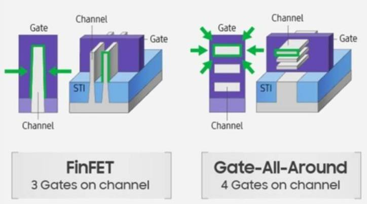 The difference between the FinFET structure adopted by TSMC (left) and the GAA structure being developed by Samsung. GAA increases the contact area between the channel and the gate to four sides, theoretically resulting in less leakage current than FinFET. / Photo by Samsung Electronics Blog
The strength of the GAA structure lies in its superior performance compared to FinFET. At the 'Samsung Foundry Forum 2021' online event in October last year, Samsung explained, "The 3nm process applying Samsung's proprietary GAA technology 'MBCFET' improves performance by 30% and reduces power consumption by 50% compared to the existing FinFET-based 5nm process."
However, there are also clear drawbacks. GAA increases the complexity of the semiconductor structure more than FinFET, which risks producing more defective products. In other words, yield may decrease. TSMC also plans to use FinFET up to 3nm for stable mass production yield and gradually introduce GAA afterward.
◆Samsung: "If GAA yield is secured, it will be a winning move"
For Samsung to succeed in mass-producing GAA-based 3nm earlier than competitor TSMC, cooperation from U.S. companies is essential. Precise technology owned by U.S. semiconductor equipment companies is required to manufacture complex transistor structures without damaging components. For example, Lam Research, one of the world's largest semiconductor equipment manufacturers in the U.S., has decided to install its latest equipment in Samsung's production lines. The next-generation 3nm wafer is thus a joint product of Korea-U.S. technology.
Samsung also expressed its ambition to strengthen foundry competitiveness by focusing investment on next-generation technology. In an investment plan announced on the 24th titled "Samsung's Future Preparation for Dynamic Innovation Growth," Samsung stated, "If Samsung's foundry business grows to No. 1 in the world, it will have an economic effect similar to having a company larger than Samsung newly established domestically." It emphasized, "We aim for 3nm mass production in the first half of this year, and securing GAA process yield can be a winning move that instantly narrows the technology gap with competitors."
© The Asia Business Daily(www.asiae.co.kr). All rights reserved.
![Clutching a Stolen Dior Bag, Saying "I Hate Being Poor but Real"... The Grotesque Con of a "Human Knockoff" [Slate]](https://cwcontent.asiae.co.kr/asiaresize/183/2026021902243444107_1771435474.jpg)


