Institute for Basic Science, Potential Use of Next-Generation Semiconductor Materials
[Asia Economy Reporter Kim Bong-su] Domestic researchers have developed a new two-dimensional carbon allotrope that can be used as a material for next-generation semiconductors.
The research team led by Lee Hyo-young, Deputy Director of the Nano-Structure Physics Research Group at the Institute for Basic Science (IBS) and professor at Sungkyunkwan University, announced on the 19th that they have developed a new two-dimensional carbon allotrope with semiconductor properties called ‘Hollygraphyne.’ By synthesizing a material that compensates for the shortcomings of graphene, which is difficult to implement as a semiconductor, the team expects it to be utilized in various fields such as optoelectronics, catalysis, and sensors.
Representative carbon allotropes include diamond and graphite. Various carbon allotropes discovered in modern times, such as graphene, fullerene, and carbon nanotubes, have revolutionized nanomaterial science. In particular, graphene’s electron mobility is 140 times that of silicon, and its strength is 200 times that of steel, making it a dream material. However, graphene lacks a bandgap, limiting its use as a semiconductor. A bandgap is necessary to sometimes allow and sometimes block the flow of electricity, enabling semiconductor functionality. To overcome graphene’s limitations, active research is underway to find new types of two-dimensional carbon allotropes that have both fast charge mobility and tunable bandgaps.
Studies have also shown that creating holes in graphene through physical and chemical methods can control the bandgap by obstructing current flow. This material is called ‘holey graphene.’ However, holey graphene has difficulty achieving desired properties because the size and distribution of the ‘holes’ are not uniform.
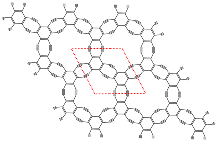
The research team applied a method of synthesizing carbon materials from the atomic level to create holes in a regular pattern, rather than making holes in existing graphene. They named the synthesized material ‘Hollygraphyne.’ Hollygraphyne is characterized by benzene rings (rings made of six carbon atoms) connected alternately by triple bonds (C≡C), and it consists of a pattern of hexagonal and octagonal rings in equal proportions.
The team synthesized ultrathin two-dimensional semiconductor Hollygraphyne at the interface of two solvents composed of water and dichloromethane, using a six-step reaction with the monomer ‘1,3,5-tribromo-2,4,6-triethylbenzene.’ Hollygraphyne’s bandgap is 1.1 eV, similar to silicon’s bandgap (1.12 eV). Additionally, its charge mobility is comparable to graphene’s (predicted to be 104 cm2V-1s-1 by calculation), confirming its suitability as a semiconductor material. Hollygraphyne’s excellent semiconductor properties and its triple bond and conjugated bond structure suggest it can be applied in various fields such as optoelectronics, catalysis, and sensors.
Deputy Director Lee Hyo-young said, “This research achievement presents the possibility of designing and synthesizing a new type of two-dimensional carbon allotrope by synthesizing ultrathin single crystals for the first time,” adding, “It will contribute to opening the era of next-generation semiconductors beyond silicon through carbon allotrope research.”
The research results were published online on the 19th in 'Matter (IF 15.589),' a sister journal of Cell.
© The Asia Business Daily(www.asiae.co.kr). All rights reserved.
![Clutching a Stolen Dior Bag, Saying "I Hate Being Poor but Real"... The Grotesque Con of a "Human Knockoff" [Slate]](https://cwcontent.asiae.co.kr/asiaresize/183/2026021902243444107_1771435474.jpg)


