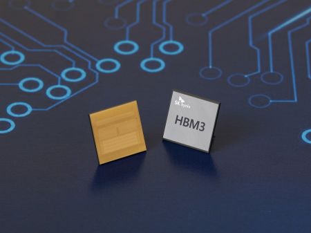
[Asia Economy Reporter Jeong Hyunjin] SK Hynix has developed the industry's first 'HBM3,' the highest-spec DRAM currently available. This product, used in high-performance data centers, is an ultra-high-speed DRAM capable of processing 163 full HD movies of 5GB capacity in one second.
On the 20th, SK Hynix announced that it developed HBM3 just 1 year and 3 months after starting mass production of HBM2E DRAM, which improved some performance aspects of the 2nd generation HBM, in July last year. HBM is a high value-added, high-performance product that vertically connects multiple DRAM chips to significantly increase data processing speed compared to conventional DRAM, and is used in supercomputers for fields such as artificial intelligence (AI) and machine learning.
HBM has been developed in the order of 1st generation (HBM) → 2nd generation (HBM2) → 3rd generation (HBM2E), and the current HBM3 is the 4th generation product of HBM. Since launching the world's first HBM DRAM in 2013, SK Hynix has accelerated HBM technology development. SK Hynix explained, "With this HBM3, we have achieved the highest speed and largest capacity among all HBM DRAMs released so far, as well as significantly improved quality levels."
HBM3 can process 819GB of data per second. This corresponds to processing data equivalent to 163 full HD movies of 5GB capacity in just one second. Compared to the previous generation HBM2E, the speed has increased by about 78%, and compared to DDR4 DRAM, the data processing speed is 33 times faster, and 16 times faster than DDR5. This product includes an error correction code (ECC) that can autonomously correct errors in data delivered to DRAM cells.
The new HBM3 will be released in two capacities: 16GB and 24GB. Notably, 24GB is the industry's largest capacity. To achieve 24GB, SK Hynix engineers ground a single DRAM chip to about 30 micrometers (μm) in height, which is one-third the thickness of an A4 sheet of paper, and vertically connected 12 of these chips using TSV technology. TSV technology is an interconnection technology that drills thousands of tiny holes in DRAM chips and connects the holes of the upper and lower chips vertically with electrodes.
Going forward, HBM3 is expected to be installed in high-performance data centers and applied to supercomputers used for machine learning that enhances AI completeness, climate change analysis, and new drug development. Mass production is expected to begin around mid-next year, coinciding with the launch of systems supporting HBM3 DRAM.
Chaseon Yong, Vice President of SK Hynix (Head of DRAM Development), said, "We will continue to solidify our leadership in the premium memory market and do our best to enhance customer value by supplying products that comply with ESG (environment, social, governance) management."
© The Asia Business Daily(www.asiae.co.kr). All rights reserved.


