UNIST Professor Jongwon Lee's Team and Dr. Jooyeon Jeong's Team at KIMM
"Amplifying Detection Signals in Infrared Spectroscopic Analysis"
[Asia Economy Reporter Kim Bong-su] A metamaterial that can increase the sensitivity of component analysis technology using infrared rays by more than one hundred times has been developed. The principle helps amplify the characteristic signals of substances included in the inspection target to make detection easier. It is expected to be applied to the detection of various biomolecules and harmful substances, which can be mass-produced and manufactured at low cost.
Ulsan National Institute of Science and Technology (UNIST) announced on the 31st that Professor Jongwon Lee's team from the Department of Electrical and Electronic Engineering, in collaboration with Dr. Juyeon Jeong's research team from the Korea Institute of Machinery and Materials, developed a metamaterial that enhances the detection signal of infrared spectroscopy, which analyzes sample components by irradiating light (infrared rays). It is a special functional material with ultra-fine structures smaller than the wavelength of light arranged on the surface, and by optimizing the design of the ultra-fine structures, the research team reported achieving a signal amplification effect more than three times better than existing technologies.
By utilizing the characteristic that material molecules absorb only specific frequencies of infrared rays (molecular fingerprint), the pattern of reflected light can be read to identify the types of substances included in the sample. However, when the substance to be detected is present in an extremely small amount in the sample, the difference in light intensity, which is the detection signal, is almost nonexistent, making it difficult to read. When light with an intensity of 1 is irradiated on a single molecular layer, only about 0.003 is absorbed.
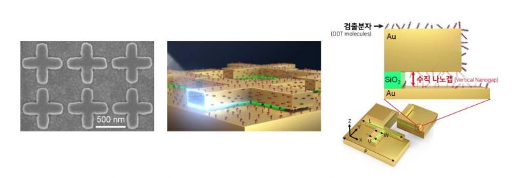
Using the developed metamaterial, the mid-infrared absorption of a single molecular layer can be increased to 0.36 (a reflection difference or absorption difference of 36%). This performance is more than 120 times improved compared to when there is no metamaterial (based on infrared reflection absorption spectroscopy), and more than three times better than existing metamaterial-based technologies. The experiment verifying the developed technology used ODT (1-octadecanethiol) molecular substance as the detection molecular sample.
This technology uses the near-field enhancement effect, where the microstructure on the metamaterial surface collects the energy of light (absorption) and then irradiates it onto molecules at once, increasing the amount of light absorbed by the molecules. The research team further enhanced the near-field intensity and designed microstructures that expose the detection molecules to the near field as much as possible to amplify the detection signal effect.
The microstructure forms a cross shape stacked in the order of metal-insulator-metal. The thickness of the insulator in the center is 10 nanometers (nm, 10^-9 m), which is thin enough to create a stronger near-field effect between the upper and lower metal layers. Also, through a vertical gap structure (the spacing between metal layers) made by carving only the insulator inward, the detection molecules can be maximally exposed to the near field. This is because molecules can enter the space carved into the insulator.
Inyong Hwang, a researcher in the Department of Electrical and Electronic Engineering at UNIST, explained, "The developed metamaterial achieved a record detection signal of 36% reflection difference in a single molecular layer detection experiment with a thickness of 2.8 nanometers (nm)," adding, "It is the highest record in single molecular layer detection experiments."
In particular, the developed metamaterial is easy to mass-produce and the manufacturing process is inexpensive. Existing metamaterials required expensive high-resolution beam lithography to create microstructures on the surface, but the developed metamaterial can be manufactured using a simple nano imprinting process and dry etching process.
Dr. Juyeon Jeong from KIMM explained, "After thinly stacking metal-insulator-metal in order, the metal and insulator on top can be peeled off into the desired shape using the nano imprinting process," adding, "By adding a dry etching process that carves the insulator, metamaterials with arranged microstructures can be mass-produced."
Professor Jongwon Lee said, "This is the first study to create a vertical gap structure that simultaneously solves the problems of near-field intensity enhancement and near-field exposure," and added, "It will be widely applied to sensor technologies that detect biomolecules, harmful substances, gases, etc. using infrared rays."
The research results were published on the 13th in the international academic journal Small Methods, published by Wiley, and are forthcoming.
© The Asia Business Daily(www.asiae.co.kr). All rights reserved.
![Clutching a Stolen Dior Bag, Saying "I Hate Being Poor but Real"... The Grotesque Con of a "Human Knockoff" [Slate]](https://cwcontent.asiae.co.kr/asiaresize/183/2026021902243444107_1771435474.jpg)


