Korea Electrotechnology Research Institute Team Completes Development of Silicon Carbide Defect Inspection Technology
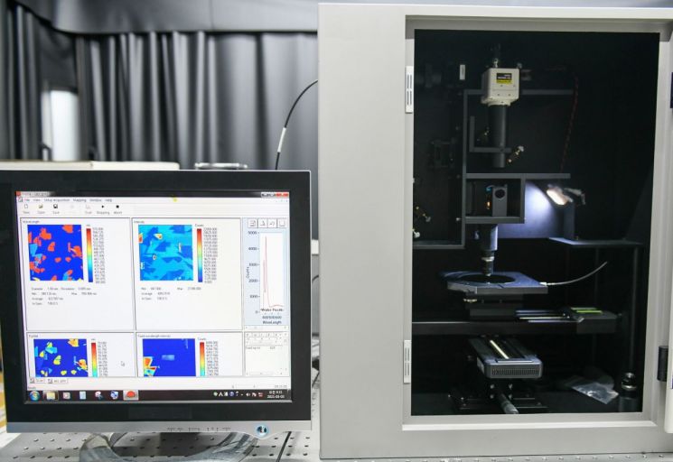 Defect analysis equipment for SiC materials used in power semiconductors. Photo by Korea Electrotechnology Research Institute (KERI).
[Asia Economy Reporter Kim Bong-su] It has become possible to domestically produce Japanese-made power semiconductor inspection equipment, which dominates 80% of the global market. This provides another foothold for counterattacks in the ongoing materials, parts, and equipment war with Japan.
The Korea Electrotechnology Research Institute (KERI) announced on the 8th that a research team led by Dr. Bang Wook and Dr. Na Moon-kyung at the Power Semiconductor Research Center developed a technology that can analyze and evaluate defects in silicon carbide (SiC) materials?the starting point of power semiconductor devices?at an early stage.
Power semiconductors are essential industrial components used wherever power is needed, playing a role similar to muscles in the human body by controlling current direction and power conversion. They are advanced materials forming the foundation of eco-friendly industries such as electric vehicles and renewable energy, and are recognized as core technologies driving the digital-based 4th industrial revolution, including 5G mobile communication networks. In particular, they are essential components in high-performance inverters connecting batteries and electric motors in electric vehicles, attracting significant attention recently.
The material maintaining the core control efficiency of power semiconductors is shifting from traditional silicon (Si) to silicon carbide (SiC). SiC, with excellent thermal and electrical properties, boasts superior durability, versatility, operating temperature and speed, and high efficiency, rapidly replacing the existing silicon power semiconductor market.
However, SiC materials inherently contain invisible internal crystal defects (dislocations), which are one of the main causes of performance degradation in semiconductor devices. These crystal defects are highly complex and difficult to identify, sometimes degrading device characteristics from the initial operation stage, and in more severe cases, causing gradual changes during use that lead to problems. For example, if issues arise in SiC power semiconductors in sensitive power system sites or electric vehicles driving on roads, it could result in serious human and property damage.
Therefore, while developing high-performance SiC power semiconductors is important, it is essential to have inspection and analysis technologies that detect defects and resolve various issues to prevent future problems. Since SiC defects are invisible and the material is very hard, observation methods are extremely challenging. Currently, Japanese-made SiC material inspection equipment holds over 80% of the global market due to the high technical difficulty and entry barriers. The equipment is also expensive, so domestic inspections are limited to performance checks on some wafer samples.
The research team developed Korea’s first technology to detect defects in SiC materials using photoluminescence (PL) phenomena. PL analysis examines the light emitted at specific wavelengths when excited electrons return to their original state. In other words, ultraviolet (UV) energy is applied to the SiC material, and the specific wavelengths emitted by electrons are analyzed to determine whether there are crystal defects.
SiC is originally an indirect bandgap semiconductor with low PL emission efficiency, making signal detection by equipment difficult. However, through collaboration with EtaMax Co., Ltd., a specialist in optical inspection equipment, the research team reduced PL loss and succeeded in developing ‘SiC material defect analysis equipment for power semiconductors.’
Unlike Japanese products that use two different wavelengths of light to detect surface and internal defects depending on the inspection target and evaluation items, the KERI-developed equipment can inspect various internal defects in SiC materials without damage using only a single laser wavelength. The equipment performance, including inspection precision (defect detection capability), showed equal or superior levels. The research team expects that through technology transfer and commercialization with companies, the inspection equipment can be supplied at about half the price of Japanese products (approximately 1.4 billion KRW). The team has completed filing foundational patents related to the developed technology.
Dr. Na Moon-kyung of KERI stated, "While we have focused on fundamental research on materials and device development to capture the high-difficulty SiC power semiconductor market, we have now established an integrated production line covering ‘design-process-evaluation’ of SiC power semiconductors by developing various evaluation methods to ensure the reliability and quality of developed products." She added, "We will continue research to expand evaluation targets (such as diamond and other wide-bandgap semiconductors) and diversify and refine analysis techniques (such as Raman analysis)."
Meanwhile, according to European market research firm IHS Markit and others, the SiC power semiconductor market is expected to grow from about $700 million (approximately 780 billion KRW) last year to about $10 billion (approximately 11.4 trillion KRW) by 2030, showing an average annual growth rate of 32%.
© The Asia Business Daily(www.asiae.co.kr). All rights reserved.
![Clutching a Stolen Dior Bag, Saying "I Hate Being Poor but Real"... The Grotesque Con of a "Human Knockoff" [Slate]](https://cwcontent.asiae.co.kr/asiaresize/183/2026021902243444107_1771435474.jpg)


