Efforts Recognized for Reducing Water Usage
[Asia Economy Reporter Dongwoo Lee] Samsung Electronics has been recognized as the first semiconductor company in the industry to be certified as a 'Water Usage Reduction Site' through continuous water resource management efforts.
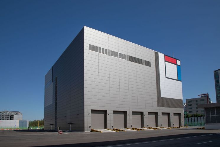
Samsung Electronics' Hwaseong Campus announced on the 22nd that it received the organizational unit 'Water Footprint' certification at the certification ceremony held by the UK-based 'Carbon Trust' at the Plaza Hotel in Seoul.
The 'Carbon Trust' is an eco-friendly certification organization established by the UK government in 2001 as part of measures to respond to climate change and reduce carbon emissions. Last year, Samsung Electronics' 5th generation (9x series) V-NAND-based '512GB eUFS 3.0' simultaneously received product-level 'Carbon Footprint' and 'Water Footprint' certifications.
The organizational unit 'Water Footprint' certification is awarded after comprehensively evaluating the amount of water used at the site and the management system for water resources over three years.
Samsung Electronics regards thorough water resource management as the starting point of environmental protection and has been practicing the 3R (Reduce, Reuse, Recycle) activities of conserving, reusing, and recycling water for over 10 years to enhance the sustainability of its semiconductor business. It has also managed water usage reduction as a business performance indicator.
The semiconductor manufacturing process uses 'ultrapure water' that contains no minerals or fine particles to ensure cleanliness and improve productivity. As semiconductor integration density increases, water usage inevitably rises.
Samsung Electronics optimized processes to minimize water usage, introduced membrane technology to purify high-concentration wastewater, and increased wastewater reuse by applying it to utility facilities. Membranes refer to films that selectively allow certain components to pass through, thereby separating mixtures.
To professionally manage water resources at semiconductor sites, Samsung employs PhD-level personnel specializing in water quality and operates over 30 technical training programs for employees to cultivate water-saving experts.
Through these efforts, Samsung Electronics Hwaseong Plant reduced water usage by approximately 1.04 million tons in 2019 compared to the 2017-2018 average of 50.15 million tons to 49.11 million tons. This amount is comparable to the water usage of a population of 200,000 people for one month.
Park Chan-hoon, Vice President and Head of Global Infrastructure at Samsung Electronics' DS Division, stated, "We will continue to discover and promote various eco-friendly ideas to ensure that the semiconductor business progresses sustainably."
Meanwhile, Samsung Electronics has made efforts to reduce energy consumption by not only managing water resources but also providing memory solutions that maximize low power characteristics, obtaining various eco-friendly certifications such as 'Carbon Footprint/Water Footprint Certification' and 'Zero Waste to Landfill Gold Certification' to expand the sustainability of its semiconductor business.
Recently, as the scope and importance of corporate social responsibility have expanded, Samsung Electronics established the Sustainability Management Office under the DS Division in July this year to build a foundation for the sustainable growth of the semiconductor business. The company plans to actively work on solving environmental and social issues going forward.
© The Asia Business Daily(www.asiae.co.kr). All rights reserved.
![Clutching a Stolen Dior Bag, Saying "I Hate Being Poor but Real"... The Grotesque Con of a "Human Knockoff" [Slate]](https://cwcontent.asiae.co.kr/asiaresize/183/2026021902243444107_1771435474.jpg)


