[Asia Economy Reporter Changhwan Lee] Samsung Electronics Vice Chairman Lee Jae-yong visited the 'Samsung Electronics Semiconductor Research Center' located in Hwaseong, Gyeonggi-do on the 19th, where he held a meeting with the Device Solutions (DS) division executives to review future semiconductor strategies, Samsung announced.
During the meeting, discussions were held on ▲next-generation semiconductor development roadmap ▲current status of memory and system semiconductor development ▲mid- to long-term strategies for equipment/materials and process technology ▲changes in the global semiconductor industry environment and post-COVID-19 measures.
Attendees included Kim Ki-nam, Vice Chairman and Head of the DS Division; Jin Gyo-young, President of the Memory Business Division; Jung Eun-seung, President of the Foundry Business Division; Kang In-yeop, President of the System LSI Business Division; Park Hak-gyu, President and Head of DS Division Management Support Office; and Kang Ho-gyu, Head of the Semiconductor Research Center.
After the meeting, Vice Chairman Lee visited researchers developing next-generation semiconductors at the Semiconductor Research Center to encourage them and reaffirmed his commitment to achieving the 'Semiconductor Vision 2030' together with the employees.
The Semiconductor Research Center is conducting research on future technologies applicable to next-generation semiconductors, including ▲advanced process and packaging technologies ▲new materials to overcome the limits of process miniaturization ▲semiconductor software research.
Vice Chairman Lee stated, "This is a harsh crisis," adding, "Our survival depends on how quickly we can make future technologies our own, and there is no time to waste."
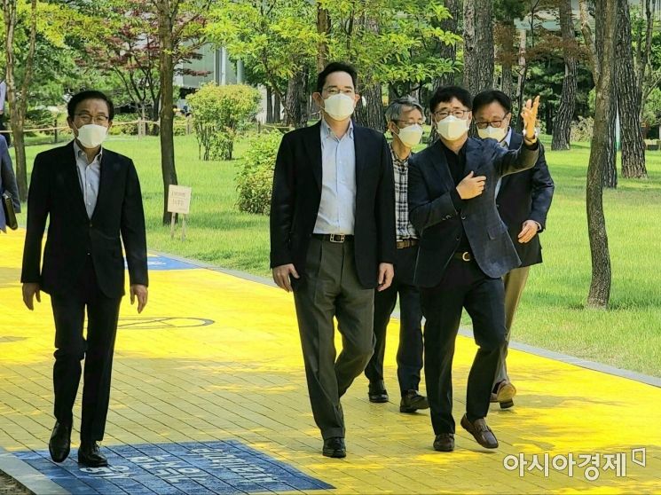 Samsung Electronics Vice Chairman Lee Jae-yong visited the 'Samsung Electronics Semiconductor Research Center' located in Hwaseong, Gyeonggi-do on the 19th, held a meeting with the Device Solutions (DS) division presidents, and reviewed future semiconductor strategies. (Photo by Samsung Electronics)
In January, as his first management activity of the year, Vice Chairman Lee visited the Semiconductor Research Center, received a report on Samsung Electronics' world-first developed 3-nanometer process technology, and urged continuous challenges toward the future.
On this day, Vice Chairman Lee also convened the heads of the Environment and Safety teams responsible for safety management at Samsung Electronics' major domestic business sites, emphasizing the importance of establishing a safe environment.
Samsung explained that this meeting was held with the purpose of fostering a strong sense of responsibility so that employees can work safely and nearby residents can live with peace of mind, as the number and scale of business sites increase and the importance of environment and safety grows.
Vice Chairman Lee urged, "The environment and safety field is the foundation for creating a sustainable future," adding, "We must systematically establish a mid- to long-term roadmap to become truly world-class in technology, safety, and environment."
© The Asia Business Daily(www.asiae.co.kr). All rights reserved.
![Clutching a Stolen Dior Bag, Saying "I Hate Being Poor but Real"... The Grotesque Con of a "Human Knockoff" [Slate]](https://cwcontent.asiae.co.kr/asiaresize/183/2026021902243444107_1771435474.jpg)


