0.1-Micrometer Ultra-Precise Alignment Achieved
Full-Scale Push Into Next-Generation HBM Packaging Market
Hanwha Semitech has successfully developed its second-generation hybrid bonder, a core technology for next-generation semiconductor packaging. This achievement comes four years after it supplied its first-generation equipment to a customer in 2022, and is expected to accelerate the company’s push into the next-generation HBM (High Bandwidth Memory) market.
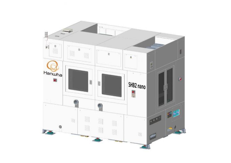
Hanwha Semitech announced on the 25th that it plans to deliver the second-generation hybrid bonder “SHB2 Nano” to a customer within the first half of this year (January to June) to conduct performance tests. The company is being evaluated as having expanded its advanced packaging equipment portfolio by securing hybrid bonding technology following its TC (thermo-compression) bonder.
A hybrid bonder is a technology that directly bonds chips to chips on copper (Cu) surfaces. It enables high stacking without bumps, which can increase data transfer speed and reduce power consumption. In particular, it can implement 16 to 20 or more layers of HBM in a thinner form, and is drawing attention as a next-generation process that will determine the performance of AI semiconductors.
The “SHB2 Nano” adopts ultra-precise alignment technology at the 0.1-micrometer (μm) level, which is about one-thousandth the thickness of a human hair. The company plans to use the development of this second-generation equipment as a springboard to make a full-fledged entry into the mass-production market in the near future.
A Hanwha Semitech representative said, “Through continuous investment in advanced technologies, we have solved the technical challenges of hybrid bonding and put the product on the right track,” adding, “This development has laid the foundation for us to lead the advanced packaging market.”
The TC bonder business is also continuing its growth trend. The “SFM5 Expert” generated more than 90 billion won in sales last year, and the company signed consecutive supply contracts in January and February this year. In the fourth quarter of last year, it successfully returned to profitability, supported by improved performance in its semiconductor division.
The company is also simultaneously developing next-generation equipment such as a second-generation TC bonder and a fluxless TC bonder. It has expanded its R&D investment as well, with last year’s semiconductor-related research and development expenses increasing by more than 50% compared with the previous year.
A Hanwha Semitech representative said, “We are responding preemptively to the rapidly changing advanced semiconductor market,” and added, “Through continuous R&D investment and innovation, we will grow into an advanced semiconductor solutions company with unrivaled technological capabilities.”
© The Asia Business Daily(www.asiae.co.kr). All rights reserved.
![Clutching a Stolen Dior Bag, Saying "I Hate Being Poor but Real"... The Grotesque Con of a "Human Knockoff" [Slate]](https://cwcontent.asiae.co.kr/asiaresize/183/2026021902243444107_1771435474.jpg)


