Expected to Power Nvidia's "Vera Rubin"
Widely Praised for Operating Speeds Surpassing Industry Standards
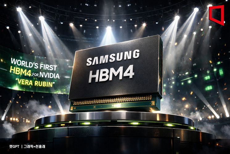
Samsung Electronics will begin mass production and shipment of the world's first sixth-generation High Bandwidth Memory (HBM4) at the end of this month. Attention is focusing on whether Samsung Electronics, which lost out to SK Hynix in the fifth-generation HBM3E race, can turn the tables and open the first chapter of its counteroffensive.
According to industry sources on the 9th, Samsung Electronics has set the timing for mass production and shipment of HBM4 to Nvidia for late February, after the upcoming Lunar New Year holiday. Earlier, during its conference call on last year's fourth-quarter earnings held on January 29, Samsung Electronics also stated that "at the request of major customers, HBM4 shipments are scheduled for February." This will be the first time in the world that next-generation HBM4 enters mass production and shipment.
HBM4 will be mounted on Nvidia's next-generation artificial intelligence (AI) chip "Vera Rubin." At Nvidia's technology conference "GTC 2026" next month, Vera Rubin equipped with Samsung Electronics' HBM4 is expected to be unveiled for the first time.
From the outset of HBM4 development, Samsung Electronics set its sights on achieving the highest performance that surpasses the standards of the Joint Electron Device Engineering Council (JEDEC), the international semiconductor standardization body. To this end, Samsung Electronics has taken a bold step by applying both 1c (10-nanometer-class sixth-generation) DRAM and a 4-nanometer foundry process to this HBM4. With this process combination, which is unique in the industry, Samsung Electronics' HBM4 achieves a data processing speed of up to 11.7 Gbps (gigabits per second), easily exceeding not only the JEDEC standard of 8 Gbps but also HBM3E at 9.6 Gbps.
Samsung Electronics' HBM4 offers a memory bandwidth of up to 3 TB/s per single stack, 2.4 times higher than its predecessor. Its maximum capacity using 12-layer stacking technology is 36 GB, and if 16-layer stacking is realized in the future, it is expected to be expandable up to 48 GB. While maximizing computing performance, its low-power design will significantly reduce power consumption and cooling costs for servers and data centers.
Samsung Electronics is currently pushing to install a new production line at its Pyeongtaek Campus Plant 4 to expand HBM production capacity. Plant 5 in Pyeongtaek, which is under vigorous construction with the goal of starting operations in 2028, is also highly likely to be operated as a "hybrid fab" that houses next-generation memory products including HBM4 and above, alongside ultra-fine foundry lines of 2 nm (1 nm = one-billionth of a meter) and below.
Ryu Hyeonggeun, a researcher at Daishin Securities, said, "Given that Samsung Electronics is receiving favorable reviews from customers for HBM4 operating speeds, it appears likely to overcome its past slump and stage a comeback," estimating this year's HBM sales at 23.7 trillion won, up 183% from the previous year.
© The Asia Business Daily(www.asiae.co.kr). All rights reserved.


