Inspection of Semiconductor Chips for Good and Defective Products Using Vision Technology
High-Speed, High-Precision Sorting into Trays
Semes, a semiconductor equipment manufacturer, announced on January 16 that it has developed the nation's first mass production equipment for large semiconductor panel-level package (PLP) sorting, called "Tepas100."
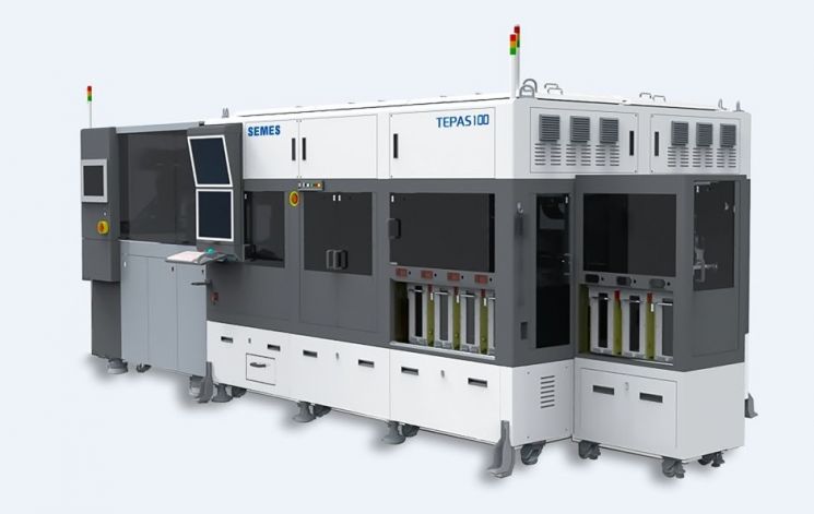
The Tepas100 is equipment that cuts raw material packages into individual units, inspects the produced semiconductor chips for good and defective products using vision technology, and sorts them into trays with high-speed and high-precision sorting technology. The significance of this equipment lies in its ability to cut and handle packages from large panels sized 515x510mm. Another feature is its compatibility with a variety of materials, ranging from organic to glass substrates.
According to the company, after cutting into packages, it has secured differentiated competitiveness in productivity and quality control by applying its proprietary "Tornado Blower" technology, which enables high-speed drying of large areas during the cleaning and drying process.
Choi Byunggab, head of the TP team, stated, "Recently, as demand for higher integration and larger sizes in semiconductor packaging increases across various applications, PLP technology utilizing large panels is gaining attention. Semes has completed its equipment lineup from legacy package and wafer-level package (WLP) to panel-level package (PLP) equipment, and plans to strengthen its position in the global semiconductor packaging market."
© The Asia Business Daily(www.asiae.co.kr). All rights reserved.
![Clutching a Stolen Dior Bag, Saying "I Hate Being Poor but Real"... The Grotesque Con of a "Human Knockoff" [Slate]](https://cwcontent.asiae.co.kr/asiaresize/183/2026021902243444107_1771435474.jpg)


