Key R&D Members Discuss Data Center Collaboration
OpenAI, the developer of ChatGPT, which is visiting South Korea to collaborate on the Stargate project-a large-scale artificial intelligence (AI) infrastructure initiative-visited the heart of Samsung Electronics, the global leader in memory production capacity.
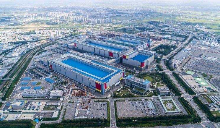
According to industry sources on October 2, after signing a Letter of Intent (LOI) with Samsung the previous day for investment in the expansion of global data centers, six core members of OpenAI's research and development (R&D) team visited the Samsung Electronics Pyeongtaek Campus.
They took commemorative photos in the office building lobby and watched a company introduction video highlighting Samsung Electronics’ history and global leadership. During the following meeting, industry insiders reported that there was an in-depth discussion about directions for future data center collaboration.
The OpenAI delegation also toured the production lines within the Pyeongtaek Campus to witness firsthand the innovative capabilities of Samsung's memory semiconductors. In particular, they were introduced to Samsung's diverse semiconductor technologies through its AI-related product portfolio, including high bandwidth memory (HBM), GDDR, high-capacity DRAM, and solid-state drives (SSD). OpenAI representatives reportedly showed great interest in Samsung’s technologies that enable next-generation AI training and inference.
The Pyeongtaek Campus serves as a core forward base supporting Samsung’s top position in global DRAM production capacity. Market research firm Omdia analyzed that, as of 2025, the Pyeongtaek Campus will account for 49% of Samsung Electronics’ DRAM wafer production, with this share expected to increase to 53% next year. CEO Sam Altman also visited the site in January last year to tour the semiconductor production lines during his trip to South Korea.
Industry experts interpreted this visit as an opportunity to confirm the practical foundation of cooperation between the two companies, while also strengthening trust in global AI infrastructure collaboration. Visiting the world’s largest semiconductor production base is also seen as a chance to further solidify confidence in Samsung’s memory capabilities.
The previous day, Samsung signed an LOI with OpenAI to cooperate on supplying 900,000 wafers per month for the Stargate project.
© The Asia Business Daily(www.asiae.co.kr). All rights reserved.


