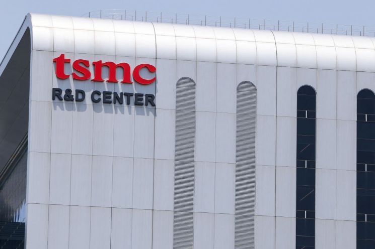
TSMC, the world's largest semiconductor foundry, will begin construction this year on a 1.4nm (nanometer, one-billionth of a meter) plant, utilizing its most advanced process technology to date.
According to Taiwanese media outlets such as Liberty Times and United Daily News on July 21, the Central Taiwan Science Park Administration under the National Science and Technology Council (NSTC) announced this plan during the 22nd anniversary ceremony held on July 18.
Director Hsu Mao-hsun of the administration explained that, upon completing the second phase of the Central Taiwan Science Park expansion, the agency officially provided land to TSMC for the construction of its state-of-the-art 1.4nm semiconductor process facility. He also noted that the administration is currently working on installing electrical and other infrastructure to support TSMC’s groundbreaking, which is scheduled for the fourth quarter of this year.
According to sources, TSMC plans to begin construction by the end of this year on four 1.4nm fabrication plants (fabs) at the site of the second-phase expansion of the Taichung complex, with a construction period of two years. The first plant (P1) aims to complete tape-out (defect checking before mass production) by the end of 2027 and to begin mass production of 50,000 wafers per month in the second half of 2028. The sources added that, with these plans, a total of 11 sub-2nm advanced fabs will be operational in Taiwan: 20 fabs at the Baoshan area of the Hsinchu Science Park in the north, 25 fabs at the Central Science Park, and 22 fabs at the Nanzih Science Park in Kaohsiung in the south.
Another source stated that TSMC’s current monthly production capacity is approximately 160,000 wafers for both 7nm and 5nm processes, and about 130,000 wafers for the 3nm process. The source further reported that TSMC expects to produce 40,000 wafers using the 2nm process by the end of this year, 100,000 wafers in 2026, and 160,000 to 180,000 wafers in 2027. The source also predicted that, once TSMC begins mass production of the 2nm process in the second half of this year, the company could become the largest producer of sub-7nm advanced processes as early as 2027.
A nanometer is a unit that refers to the width of semiconductor circuit lines. Currently, the most advanced technology in mass production is the 3nm process, utilized by both TSMC and Samsung Electronics.
© The Asia Business Daily(www.asiae.co.kr). All rights reserved.


