Notice of Demolition of Former LG Plant 2 Building in Cheongju Posted on Internal Bulletin Board
Demolition Expected to Finish by September, P&T Facility to Be Built
Potential Use as a "Test Fab"
SK Hynix is set to build its seventh semiconductor back-end process facility in Cheongju, aiming to strengthen its competitiveness.
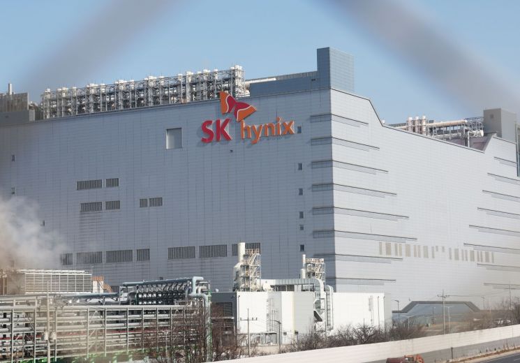
According to industry sources on June 24, SK Hynix recently announced on its internal bulletin board that it plans to demolish the building located on the site of the former LG Plant 2 in Cheongju, which it had previously acquired, in order to construct the 'P&T (Package & Test) 7' facility. The demolition is scheduled to be completed by September.
SK Hynix's P&T facilities are responsible for the semiconductor back-end process. Currently, these facilities are located in Icheon and Cheongju, and with the addition of the new facility, the total number will reach seven. The specific timing for the groundbreaking and the detailed purpose of the new back-end facility have not yet been determined. However, according to industry sources, it is highly likely to be used as a test fab.
SK Hynix appears to be aiming to strengthen its competitiveness in the semiconductor back-end process based on this plan. The semiconductor back-end process involves completing individual chips from wafers that have undergone the front-end process and packaging them into final products. As the improvement of performance through process miniaturization has recently reached its limits, the importance of packaging technology, which can overcome these limitations and enhance semiconductor performance and power efficiency, is increasingly being highlighted.
In particular, high-bandwidth memory (HBM), which is produced by stacking multiple DRAM chips, requires advanced packaging technology to address issues such as heat dissipation and warping, which become more pronounced as the number of stacked layers increases.
© The Asia Business Daily(www.asiae.co.kr). All rights reserved.


