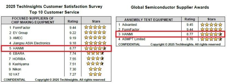
Earlier this year, Hanmi Semiconductor was named one of the "World's Top 10 Best Semiconductor Equipment Companies" in the core semiconductor equipment category, based on a survey conducted by TechInsights targeting semiconductor manufacturers worldwide. In addition, the company was recognized for its technological competitiveness by being selected as the "Best Semiconductor Equipment Company" in the assembly and test equipment sector in the evaluation of various semiconductor process fields.
Previously, Hanmi Semiconductor had demonstrated its world-class technological capabilities by being selected as one of TechInsights' "World's Top 10 Best Semiconductor Equipment Companies" for three consecutive years, from 2022 to 2024.
Hanmi Semiconductor has further strengthened its global standing by standing shoulder to shoulder with global semiconductor equipment giants such as ASML, Lam Research, and Applied Materials.
A Hanmi Semiconductor representative stated, "Being the only Korean semiconductor equipment company selected alongside global companies in the 2025 TechInsights Customer Satisfaction Survey is a testament to the excellence and reliability of our technology being recognized internationally." The representative added, "We will continue to strengthen our position as a leading semiconductor equipment technology company through relentless R&D investment and customer-centric innovation."
Founded in 1980, Hanmi Semiconductor is a global semiconductor equipment company with approximately 320 customers worldwide. Hanmi Semiconductor holds the top global market share in the TC bonder market for HBM (High Bandwidth Memory) production equipment, which is a core component of AI semiconductors. In the advanced HBM3E 12-layer production TC bonder market, the company leads the market with an overwhelming market share of over 90%.
Hanmi Semiconductor's "micro SAW&VISION PLACEMENT" has also firmly maintained the number one global market share since the mid-2000s. This flagship equipment integrates the entire process from precision cutting of semiconductor packages to cleaning, drying, high-resolution 2D/3D vision inspection, quality sorting, and automatic stacking.
TechInsights, founded in 1989 and headquartered in Ottawa, Canada, is a global semiconductor technology analysis and market research firm. It is highly trusted by high-tech companies and government agencies worldwide for its outstanding capabilities in market outlook analysis of semiconductors and electronic products, as well as chip-level circuit and process technology structure analysis.
© The Asia Business Daily(www.asiae.co.kr). All rights reserved.


