Defect Removal in Next-Generation Semiconductor Material Molybdenum Disulfide (MoS2) Using Low-Temperature Process
Compatible with BEOL Process, Facilitates Development of Smaller, Faster, Low-Power Semiconductors; Published in ACS Nano
A technology has been developed to remove defects in semiconductor materials, enabling the production of smaller, faster, and low-power chips.
The team led by Professor Kwon Jimin of the Department of Electrical and Electronic Engineering at UNIST, in collaboration with Professor Noh Yongyoung's team from the Department of Chemical Engineering at POSTECH, announced on the 25th that they have developed a technology to remove defects in molybdenum disulfide, a next-generation semiconductor material, at 200°C.
 Research team (from the bottom left counterclockwise): Dr. Haksoon Jung (first author), Professor Jimin Kwon, Dr. Yongwoo Lee, Researcher Sumin Hong, Researcher Junho Koo, Researcher Sanghyun Lee. Provided by UNIST
A single semiconductor chip, about the size of a fingernail, contains at least several billion integrated devices. Molybdenum disulfide is attracting attention in the industry as a semiconductor material that is expected to increase chip integration density and suppress leakage current, enabling the creation of low-power chips without heat generation.
The technology to remove defects that occur during the actual integration of molybdenum disulfide into chips at low temperatures is a key challenge for commercialization. This is because molybdenum disulfide is deposited on silicon devices, and the already completed silicon devices must not be damaged by heat.
The research team filled the defects at 200°C using a substance called PFBT, restoring the atomic ratio of molybdenum to sulfur in molybdenum disulfide (MoS2) to 1:1.98, close to the theoretical ratio of 1:2. During the deposition process of molybdenum disulfide in thin-film form, defects occur where sulfur atoms are missing from their original positions, resulting in an actual sulfur-to-molybdenum ratio of about 1:68. Since defects hinder the flow of electrons, these defects must be filled and the atomic ratio restored to near-theoretical levels to ensure semiconductor performance and durability.
Dr. Jung Haksoon, the first author, explained, "The biggest advantage is that defect recovery occurs at temperatures below 200°C, making it compatible with existing silicon semiconductor BEOL processes." The BEOL process is a step that connects devices already deposited on a substrate and is conducted below 350°C to prevent device damage.
PFBT (pentafluorobenzenethiol), used in the recovery step, has a hexagonal benzene ring structure with a thiol group (-SH) and fluorine (F) attached. The sulfur in the thiol group directly fills the defect, while the fluorine guides the molecule to the sulfur defect and then helps separate the remaining parts of the molecule except for the sulfur. The research team confirmed the feasibility of this chemical reaction through molecular dynamics simulations. Furthermore, X-ray spectroscopy analysis showed that the actual sulfur vacancies were filled at low temperatures.
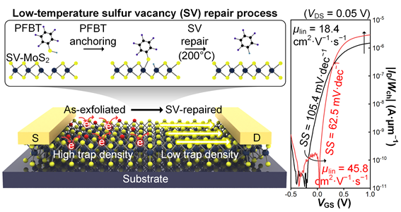 Low-temperature sulfur defect recovery process and electrical performance improvement through adsorption and desorption of PFBT.
When a transistor device was fabricated using molybdenum disulfide with defects filled, the charge mobility improved by 2.5 times compared to the case with defects. The faster the charge mobility, the faster the device can operate. The subthreshold swing value, an indicator of power consumption, also decreased by about 40%.
Professor Kwon Jimin said, "Sulfur defects generated during processing are a major issue in semiconductor devices targeting advanced nanoscale nodes. Through the developed low-temperature sulfur defect recovery technology using organic molecules, we plan to further expand research on defect recovery and interface property improvement not only for molybdenum disulfide but also for various next-generation semiconductor materials."
This research was conducted with Dr. Jung Haksoon of UNIST and researcher Kim Mingyu of POSTECH's Department of Chemical Engineering as first authors, and was supported by the National Research Foundation of Korea (NRF) under the Ministry of Science and ICT, the Institute for Information & Communications Technology Planning & Evaluation (IITP), and Ulsan National Institute of Science and Technology.
The research results were officially published on February 18 in ACS Nano, a prestigious international journal in the field of nanoscience and technology.
© The Asia Business Daily(www.asiae.co.kr). All rights reserved.


