Real Semiconductor Glass Substrate Displayed at CES 2025
Potential Use as Core Material for AI Data Centers Suggested
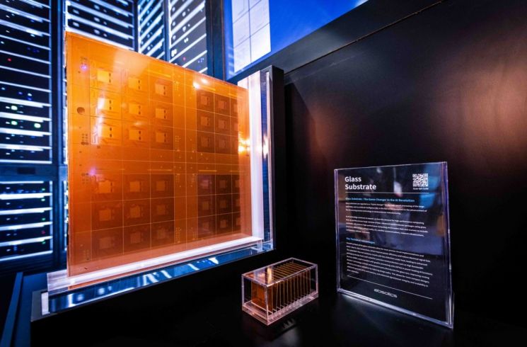
SKC will showcase glass substrates, regarded as a 'game changer' in the semiconductor industry, at CES 2025, the world's largest industrial exhibition, held in Las Vegas, USA, from the 7th to the 10th (local time).
SKC will exhibit the glass substrates in the AI DC (AI Data Center) zone within the exhibition hall jointly operated by four SK Group affiliates (SKC, SK Hynix, SK Telecom, and SK Enmove). The SK exhibition hall, themed "Innovative AI·Sustainable Tomorrow," is composed of three zones: AI DC, AI Services, and AI Ecosystem.
At this exhibition, the glass substrates will be introduced as a solution to boost the speed of AI servers that process large-scale data. The application of glass substrates in AI data centers will be demonstrated so that visitors can experience the actual utilization of the substrates.
In addition to the exhibition, a presentation explaining the excellence of the glass substrates is scheduled. Absolics, an investor in SKC’s glass substrate business, will participate in a presentation titled "Cutting-edge Hardware and Software for AI Semiconductors," proposing the development direction of evolving AI solutions through glass substrate technology.
Glass substrates have the advantage of enabling ultra-fine circuit implementation and embedding various components such as MLCC (Multilayer Ceramic Capacitors) internally, allowing large-capacity CPUs and GPUs to be mounted on the surface. This results in a 40% faster data processing speed compared to conventional substrates, while power consumption and package thickness are reduced by more than half. Applying glass substrates to AI data centers can drastically reduce the center’s area and power usage.
SKC has become the world’s first to complete a mass production plant in Georgia, USA, and is accelerating commercialization. Last year, it secured production subsidies of $75 million (approximately 109.1 billion KRW) and R&D subsidies of $100 million (approximately 145.5 billion KRW) from the U.S. government in recognition of its technological innovation.
An SKC official said, "As the world’s first company to commercialize semiconductor glass substrates, we are able to once again showcase our technological excellence to the world at this CES. We will solidify our technological superiority in the increasingly fierce semiconductor competition through glass substrates."
© The Asia Business Daily(www.asiae.co.kr). All rights reserved.
![Clutching a Stolen Dior Bag, Saying "I Hate Being Poor but Real"... The Grotesque Con of a "Human Knockoff" [Slate]](https://cwcontent.asiae.co.kr/asiaresize/183/2026021902243444107_1771435474.jpg)


