Professor Oilkwon’s Team Develops New Amorphous Quasicrystal Surpassing Metal Limits
Expected to Mark a Crucial Turning Point in Semiconductor Miniaturization
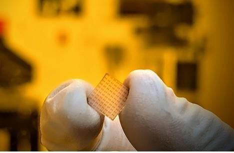 A semiconductor device applying a new amorphous quasi-metal nanometer-scale ultrathin material developed by Professor Oilkwon Oh's team at Ajou University. As the semiconductor industry requires metals with lower resistivity due to the miniaturization of semiconductor devices, this is expected to be utilized as a new core technology leading future advancements. Photo by Ajou University
Domestic researchers have opened a technological breakthrough to overcome the physical limits encountered in the miniaturization process of semiconductor manufacturing.
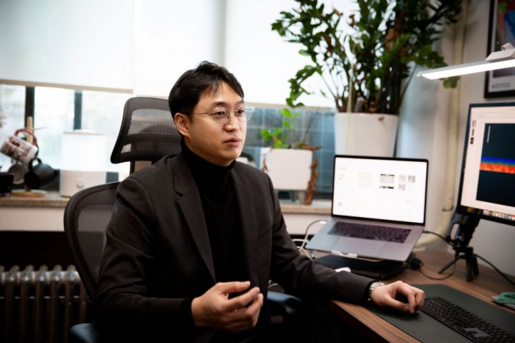
Ajou University announced on the 3rd that Professor Oilkwon’s team has developed the world’s first amorphous quasi-metal nanofilm material with properties completely opposite to those of conventional metals. The research was published in the January issue of the globally renowned journal Science.
The newly developed material exhibits technological features that surpass the limitations of conventional metals. Conventional metals face a problem where the probability of electron collisions increases as the thickness of the thin film decreases, causing a sharp rise in resistivity.
However, the phase quasi-metal material developed this time has an innovative characteristic where resistivity decreases as the thickness becomes thinner. The research team believes this technology can overcome the difficulties semiconductor industries face as circuit linewidths rapidly shrink to sizes below 2 nanometers.
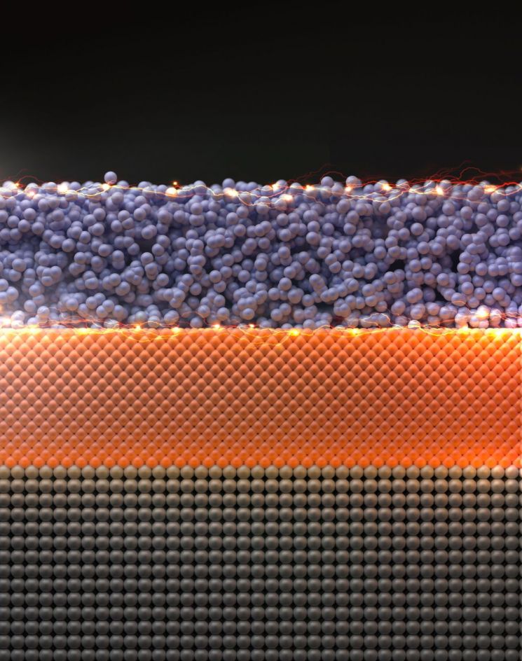 An illustration describing the new amorphous quasi-metallic nano-ultrathin material developed by the joint research team at Ajou University. It shows a sapphire crystal layer (brown) and an Nb crystal layer (orange) with an amorphous NbP layer (purple) on top. Image source=Science
Metal wiring in semiconductors is an essential process connecting unit transistors within a chip. High conductivity and low resistivity are required. However, copper (Cu), currently in use, and alternative materials such as molybdenum (Mo) and ruthenium (Ru) all have the limitation of increased resistivity due to thickness constraints. The material developed in this study suggests the possibility of solving these problems and is expected to contribute to the advancement of miniaturization technology in the semiconductor industry.
There is also the advantage of enabling semiconductor processes to be configured at a lower cost. This material can be realized in an amorphous state without a separate complex heat treatment process, and its low growth temperature facilitates integration with existing processes. This is significant because it can greatly reduce the huge initial cost burden required to replace or supplement existing semiconductor processes.
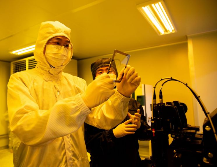 Checking the mask pattern for the fabrication of semiconductor devices based on topological semimetals. Photo by Ajou University
Professor Oh’s team collaborated with researchers from Stanford University in the United States to synthesize the material and study its electrical properties. The material is evaluated to have high compatibility with existing semiconductor technologies even in low-temperature processes, making commercialization highly feasible. In particular, it can be realized in an amorphous form without additional high-temperature heat treatment, offering excellent cost efficiency.
The Ajou University research team is developing a phase quasi-metal process based on atomic layer deposition (ALD) as a follow-up study. This allows control of thin film thickness at the atomic level, making it suitable for more precise semiconductor manufacturing and is regarded as a step closer to commercialization.
Professor Oh said, "This research is significant as it experimentally proves a new material that has never been attempted before," and added, "This new concept metal material will be a breakthrough to overcome the limits of semiconductor technology."
© The Asia Business Daily(www.asiae.co.kr). All rights reserved.


