R&D Equipment Introduction Ceremony at Giheung NRD-K Today
NRD-K is a State-of-the-Art Integrated R&D Complex
20 Trillion Won Investment by 2030
Established in Giheung, the Birthplace of Samsung Semiconductor
Largest R&D Cluster Connecting Giheung-Hwaseong-Pyeongtaek
Jeon Young-hyun, Vice Chairman and Head of Samsung Electronics Device Solutions (DS) Division, stated at the 'Next-Generation Semiconductor Research & Development (R&D) Complex New Research & Development - K (hereinafter NRD-K) Equipment Installation Ceremony' held on the 18th at the Giheung Campus in Yongin, Gyeonggi Province, "Through NRD-K, we will drastically improve development speed by establishing a virtuous cycle system from fundamental research of next-generation semiconductor technology to mass production of products."
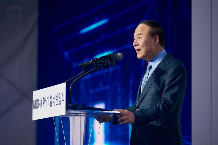 On the 18th, Vice Chairman Jeon Young-hyun delivered a commemorative speech at the NRD-K equipment installation ceremony held at Samsung Electronics Giheung Campus. Photo by Samsung Electronics
In his commemorative speech, Jeon said, "We will lay the foundation for a new leap forward in Giheung, where Samsung Electronics' 50-year semiconductor history began, and create the future for the next 100 years."
NRD-K is a state-of-the-art integrated research and development complex spanning 109,000㎡ (approximately 33,000 pyeong) that Samsung Electronics is constructing to secure future semiconductor technologies. The total investment is expected to reach 20 trillion KRW by 2030.
The fact that NRD-K is being built in Giheung is also significant. The Giheung Campus is a symbolic site where Samsung Electronics officially began its semiconductor business following the Tokyo Declaration in February 1983. Starting with the construction of the mass production line in September 1983, Samsung's advanced VLSI-grade semiconductor business was born here. In 1992, Samsung developed the world's first 64M DRAM, achieving the number one position in the DRAM market, and in 1993, it became the driving force laying the foundation for 30 years of leadership in the memory semiconductor sector. Currently, the campus operates foundry (semiconductor contract manufacturing) 8-inch and 12-inch lines, LED lines, and more, covering an area of about 440,000 pyeong.
Samsung Electronics plans to establish NRD-K, the core of future technology research, in Giheung to create a turning point for innovation and maximize synergy between technology and organizations. NRD-K is expected to become the heart of semiconductor technology, solidifying technological competitiveness as the largest semiconductor R&D cluster in the Seoul metropolitan area, connecting Giheung, Hwaseong, and Pyeongtaek. Specifically, it will be equipped with advanced infrastructure to serve as a core research base across all semiconductor fields, including memory, system semiconductors, and foundry, enabling fundamental technology research and product development to be conducted in one place.
Samsung Electronics expects NRD-K to play a pivotal role in next-generation memory semiconductor development by introducing cutting-edge production equipment such as high-resolution EUV lithography systems and new material deposition equipment, as well as wafer bonding infrastructure that implements innovative structures by bonding two wafers together. With the establishment of NRD-K, Giheung is anticipated to become a central hub of the advanced semiconductor industry ecosystem. Samsung Electronics also plans to further expand R&D cooperation with partner companies.
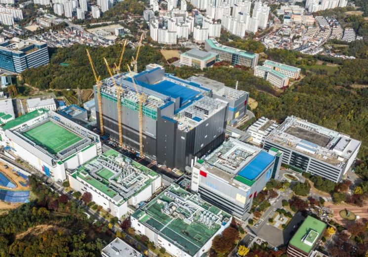 NRD-K, the next-generation semiconductor R&D complex at Giheung Campus. Photo by Samsung Electronics
About 100 people attended the event, including Vice Chairman Jeon, key executives of the DS Division, representatives of equipment partner companies, and employees of the Semiconductor Research Institute. Park Kwang-sun, Head of Applied Materials Korea, stated, "At a time when a win-win partnership is more important than ever, Applied Materials will do its best to contribute to the advancement of the semiconductor industry by accelerating innovation together through close cooperation with Samsung Electronics."
Meanwhile, amid fierce global semiconductor supremacy competition, Samsung Electronics is striving to attract production lines to its home country and actively encouraging the establishment of research institutes. The origin of Samsung Electronics Semiconductor Research Institute dates back to the 'Semiconductor R&D Center' established in 1982. In 1983, another center was established at the Bucheon plant. Since then, Samsung's R&D lines have evolved through the M line, U line, and RS line, and in 2006, the NRD (New Research & Development) line was established at the Hwaseong Campus to continuously secure a competitive edge in next-generation semiconductor technology. The NRD line currently serves as the main base for semiconductor research and development.
Additionally, Samsung Electronics invested a record quarterly amount of 8.87 trillion KRW in R&D in the third quarter. The company is also fully committed to securing future technological competitiveness by expanding advanced packaging facilities and more.
© The Asia Business Daily(www.asiae.co.kr). All rights reserved.


