Semes, a semiconductor equipment company, announced on the 21st that it has developed and mass-produced Korea's first plasma-type semiconductor dry cleaning equipment (equipment name PURITAS).
Due to the miniaturization and high integration trend of semiconductor patterns (microcircuits), there are limitations in the process with the existing wet cleaning method. The equipment, manufactured using a dry cleaning method, uses remote plasma instead of direct plasma on the wafer, enabling highly selective cleaning and etching of various film types, significantly improving productivity, the company explained.
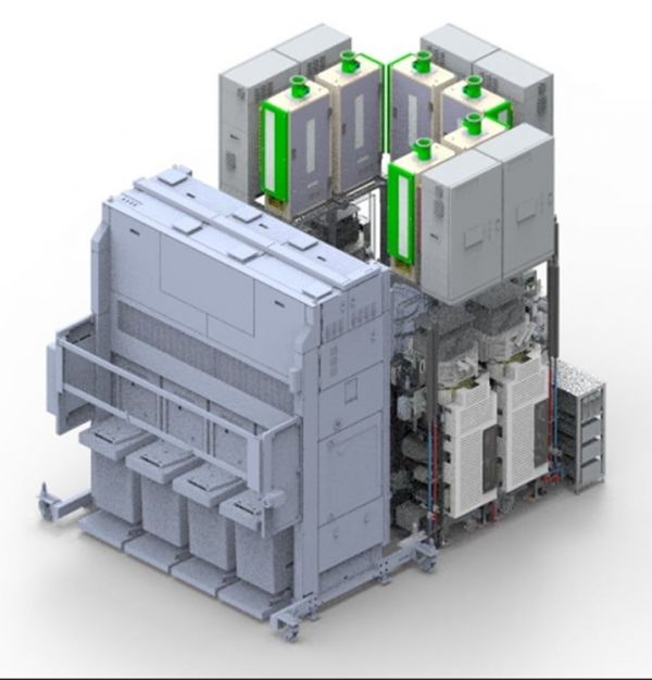
By using only radicals (neutral particles) that cause chemical reactions without using ions that damage the substrate, highly selective side etching is possible, making it essential for the production of next-generation devices such as 3D-DRAM, CFET, and GAA modules. Currently, leading equipment manufacturers produce gas-type dry cleaning equipment.
Choi Gil-hyun, CTO, said, "Starting with the shipment of the first mass-produced unit this year, we expect demand to increase as the transition to 3D products (memory and logic) progresses, and we will secure leadership in the dry cleaning market."
© The Asia Business Daily(www.asiae.co.kr). All rights reserved.
![Clutching a Stolen Dior Bag, Saying "I Hate Being Poor but Real"... The Grotesque Con of a "Human Knockoff" [Slate]](https://cwcontent.asiae.co.kr/asiaresize/183/2026021902243444107_1771435474.jpg)


