Gauss Labs Releases 'Panoptes VM' 2.0
SK Hynix Applies It to Etching Process Creating Semiconductor Circuit Patterns
Gauss Labs, an industrial artificial intelligence (AI) company invested in by SK Hynix, announced on the 13th the release of version 2.0 of its AI-based virtual metrology solution, 'Panoptes VM.' SK Hynix plans to introduce this solution to the etching process following its application in the thin film deposition process.
Semiconductor metrology refers to the process of measuring whether the physical and electrical characteristics of semiconductor devices meet the required standards at each stage of semiconductor manufacturing to improve productivity. By applying the Panoptes VM solution, it is possible to predict the process results of all products without physical full-scale measurement, significantly reducing time and resources.
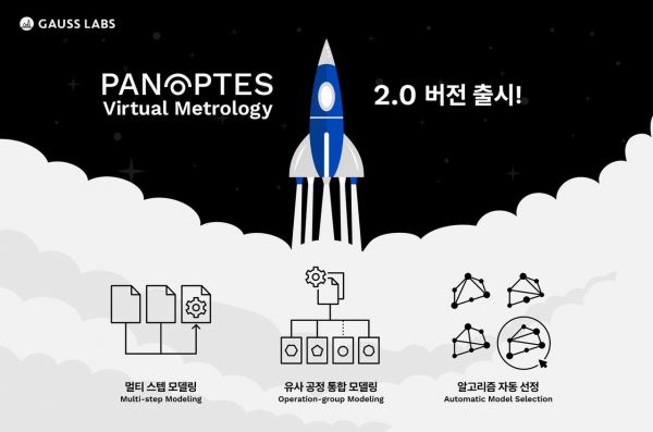
The newly released Panoptes VM 2.0 features new modeling functions that greatly improve prediction accuracy and usability compared to the previous version.
SK Hynix has decided to expand the application of the enhanced Panoptes VM 2.0 to the etching process. Etching is the process of selectively removing unnecessary parts using liquid or gaseous etchants on a wafer to create semiconductor circuit patterns.
Gauss Labs launched Panoptes VM 1.0 in November 2022. SK Hynix introduced this solution to its mass production fab starting in December of the same year, applying it to the 'thin film deposition' process. Thin films are very thin coatings formed on substrates such as insulated semiconductors, glass, or ceramics, applied through physical and chemical reactions using processes like vacuum deposition or sputtering on wafers. The thickness and refractive index of the thin film are directly linked to the quality of semiconductors.
Through Panoptes VM, SK Hynix linked the virtual metrology results with APC (Advanced Process Control, a solution that finds optimal equipment process conditions), improving process variation (quality fluctuation range) by about 29% and achieving yield enhancement.
Gauss Labs added a 'multi-step modeling' function to this solution. This function allows modeling by utilizing data from both the process to be predicted and the preceding processes. Applying this function to the etching process, which is heavily influenced by previous processes, can increase the accuracy of virtual metrology.
The Gauss Labs technical team also added a 'similar process integrated modeling' function, which integrates data from similar processes to minimize issues caused by data scarcity, and an 'automatic algorithm selection' function that automatically chooses the optimal prediction algorithm based on data characteristics, improving both virtual metrology quality and user convenience.
Kim Young-han, CEO of Gauss Labs, said, "Our efforts over the past four years have produced meaningful results in the semiconductor field, known as the most precise manufacturing industry. Based on the industrial AI technology gained here, we will pioneer the global market."
© The Asia Business Daily(www.asiae.co.kr). All rights reserved.


