A p-type semiconductor material and a thin-film transistor utilizing it, which will overcome the limitations of semiconductor fine processes and lead innovation in the semiconductor industry, have been developed domestically.
The Electronics and Telecommunications Research Institute (ETRI) announced on the 23rd that it has developed a p-type Se-Te (selenium-tellurium) alloy transistor based on tellurium (Te)-based chalcogenide p-type semiconductor material, which allows room-temperature deposition and has a simple process.
In particular, ETRI also developed a technology that can systematically control the threshold voltage of n-type transistors by controlling charge injection in the Te thin film within a heterojunction structure of n-type oxide semiconductor and p-type Te, thereby increasing its applicability.
Semiconductors are classified into intrinsic semiconductors and impurity semiconductors depending on doping. Among them, intrinsic semiconductors are classified as pure semiconductors without added impurities. Also, silicon, commonly used in semiconductors, does not allow electrons to move, so no current flows even when voltage is applied.
For the same reason, intrinsic semiconductors are utilized by adding specific impurities to adjust the semiconductor properties and electrical conductivity. At this time, impurity semiconductors are classified into n-type and p-type semiconductors depending on the added impurities.
The material mainly used in the display field currently is an n-type oxide semiconductor based on indium gallium zinc oxide (IGZO). Since p-type oxide semiconductors have not secured electrical characteristics and processability compared to n-type oxide semiconductors, p-type low-temperature polycrystalline silicon (LTPS) is sometimes used, but it shows limitations such as high cost and substrate size restrictions.
However, recently, as high-resolution displays (SHV level (8K*4K)) require a scanning rate of over 240Hz, industry interest has focused on the development of p-type semiconductors.
This is because it is difficult to implement high scanning rate displays with transistors based only on n-type semiconductors, which have been mainly used in existing displays. For the same reason, demand for p-type semiconductors comparable to n-type characteristics is increasing in the field.
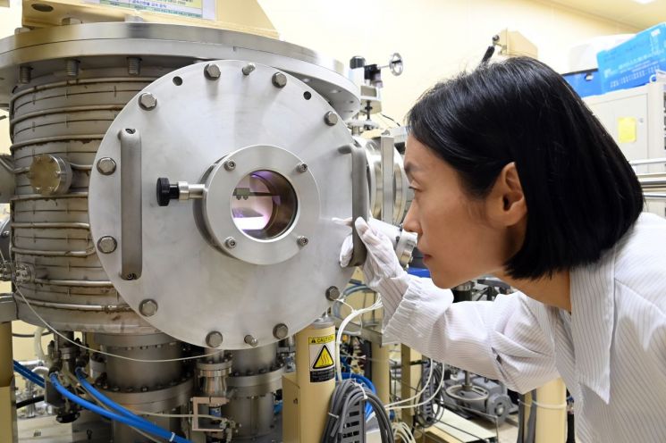 An ETRI researcher is observing the phenomenon of Te-based p-type semiconductor thin film being deposited on sputtering equipment. Photo by Electronics and Telecommunications Research Institute (ETRI)
Inspired by this, ETRI researchers developed a p-type semiconductor by adding Se to Te (raising the crystallization temperature of the channel layer), depositing an amorphous thin film at room temperature, and then crystallizing it through subsequent heat treatment. This semiconductor enables improved mobility and higher on/off current ratio characteristics compared to existing transistors.
ETRI researchers also confirmed that when the Te-based p-type semiconductor is introduced as a heterojunction structure on an n-type oxide semiconductor thin film, the electron flow of the n-type transistor can be controlled according to the thickness of Te, allowing adjustment of the threshold voltage of the n-type transistor.
In particular, by adjusting the thickness of Te in the heterojunction structure without a passivation layer, the stability of the n-type transistor was improved.
Based on these achievements, ETRI researchers expect accelerated development of the next-generation display industry that simultaneously satisfies high resolution and low power consumption.
P-type semiconductors have been confirmed to have excellent applicability not only in displays but also in the semiconductor industry.
For example, leading global semiconductor companies are currently developing fine processes to increase semiconductor integration density, but many experts analyze that the increase in semiconductor integration density has reached its limit.
Accordingly, the industry has recently been utilizing stacking methods that stack multiple semiconductor chips. Silicon Through-Silicon Via (TSV) is a representative stacking method that stacks multiple wafers and then drills holes to electrically connect them. This has the advantage of increasing space utilization on the substrate and reducing power consumption.
However, challenges such as high process costs and low yield remain to be overcome.
From this perspective, the heterojunction thin-film transistor and p-type semiconductor device based on n-type oxide semiconductor and Te-based p-type semiconductor developed by ETRI researchers operate stably even with processes below 300°C, and are evaluated as catalysts to accelerate the commercialization of M3D.
The development results were published in April and last month in the 'ACS Applied Materials & Interfaces' journal of the American Chemical Society (ACS), respectively.
Jonghaeng Cho, principal researcher at ETRI's Flexible Electronic Devices Research Lab, said, "ETRI's research results are important achievements that will be widely utilized not only in next-generation display fields such as OLED TVs and extended reality (XR) devices but also in ultra-low power complementary metal-oxide-semiconductor (CMOS) circuits and DRAM memory research."
© The Asia Business Daily(www.asiae.co.kr). All rights reserved.
![Clutching a Stolen Dior Bag, Saying "I Hate Being Poor but Real"... The Grotesque Con of a "Human Knockoff" [Slate]](https://cwcontent.asiae.co.kr/asiaresize/183/2026021902243444107_1771435474.jpg)


