'Samsung Foundry 2024' Held in Korea
Choi Si-young, Samsung Electronics President, Delivers Keynote Speech
Japanese AI Accelerator 2nm Turnkey Order
Enhanced MPW Support for Korean Fabless
"Samsung's integrated solution not only guarantees artificial intelligence (AI) and high-performance computing (HPC) performance but also maximizes customer convenience in supply chain management. By 2027, if photonics (optical device technology) is secured, we will be able to complete a 'one-stop AI solution.'"
Choi Si-young, President of Samsung Electronics Foundry Business, made these remarks as the keynote speaker at the 'Samsung Foundry Forum 2024' held on the 9th at COEX in Seoul. President Choi, who stated that Samsung Foundry's competitiveness in the AI era lies in turnkey production, expressed confidence that "a comprehensive AI solution will be the driving force for success in the AI revolution."
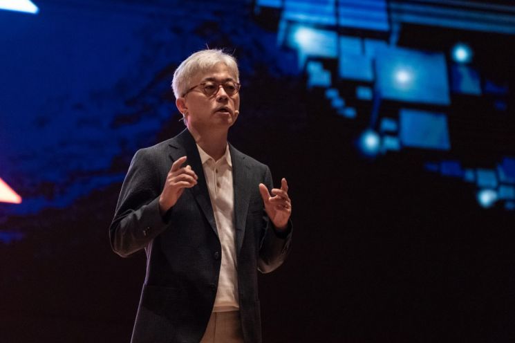 On the 9th, Choi Si-young, President of Samsung Electronics Foundry Division, delivered the keynote speech at the 'Samsung Foundry Forum 2024' held at COEX in Samseong-dong, Seoul. / Photo by Samsung Electronics
Japanese AI Accelerator 2nm-Based Turnkey Order Achievement
On the day, President Choi explained, "Despite the stagnant market environment, AI has evolved the fastest," adding, "The speed is astonishing." He continued, "For this evolution to continue without stopping, various technological innovations must be achieved," emphasizing, "Semiconductor innovation is needed more than ever."
In this situation, Samsung Electronics is enhancing its turnkey competitiveness to increase foundry business opportunities. The focus is on providing comprehensive solutions, including semiconductor intellectual property (IP), interposers, high-bandwidth memory (HBM), logic, and advanced packaging. President Choi emphasized, "Providing each solution individually is not difficult, but Samsung Electronics is the only company in the world that offers integrated solutions."
Results are already becoming visible. Samsung Electronics has secured an advanced process turnkey service in cooperation with Gaonchips, a domestic design solution provider (DSP). They plan to mass-produce a 2nm (SF2) based AI accelerator for the Japanese AI company Preferred Networks (PFN) through 2.5D advanced packaging. PFN develops software and hardware technologies not only for chips but also for supercomputers and generative AI-based models in the deep learning field.
Samsung Electronics is also enhancing advanced process technology according to its existing roadmap. Following the start of mass production of the 3nm process based on the next-generation transistor structure Gate-All-Around (GAA) in 2022, the company is currently progressing with the second-generation 3nm process. President Choi stated, "Starting with the 2nm process in 2025, we plan to offer SF2Z (2nm process based on Backside Power Delivery Network, BSPDN) in 2027," adding, "We plan to provide a 1.4nm process in 2027."
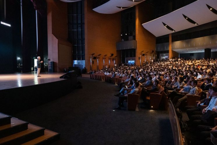 The keynote speech venue at the 'Samsung Foundry Forum 2024' held on the 9th at COEX, Samseong-dong, Seoul. / Photo by Samsung Electronics
Meanwhile, Shim Sang-pil, Vice President of Samsung Electronics Foundry Business, noted on the day, "The world is rapidly changing through AI," pointing out the pronounced shortage of HBM. He explained, "HBM is currently in such short supply that we cannot meet demand," adding, "When meeting customers, they are clamoring for HBM." He further said, "Since we cannot obtain it ourselves, we have to ask the Memory Business Division for more HBM," and added, "Demand for HBM this year has reportedly increased fourfold compared to last year."
Choi Jang-seok, Executive Director of Samsung Electronics Memory Business Division, who also participated as a presenter at the event, explained, "The 16-layer HBM4 requires not only packaging but also various cutting-edge packaging technologies, as well as new processes such as FinFET for performance, power, and area optimization. It is essential to appropriately combine and implement all these new technologies," adding, "We are preparing according to the planned schedule."
Expanding MPW Services to Support Fabless Prototype Production
Samsung Electronics also detailed plans to support the domestic system semiconductor ecosystem. President Choi said, "Samsung Electronics supports various specialty process technologies beyond advanced processes to collaborate with domestic fabless (semiconductor design) customers." He added, "Through the fusion of specialty solutions such as BCD, which improves AI power efficiency, and high-sensitivity sensor technology that enhances edge device accuracy, we will provide customers with the most necessary AI solutions."
Specialty process technology is used in processes to implement specific functions such as embedded memory and image sensors. The BCD process integrates Bipolar analog signal control, CMOS digital signal control, and DMOS high-voltage management transistors into a single chip, mainly used for power semiconductor production.
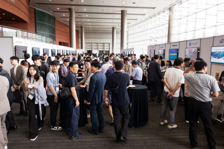 The Samsung partner company booths set up at the 'Samsung Foundry Forum 2024' held on the 9th at COEX, Samseong-dong, Seoul / Photo by Samsung Electronics
Samsung Electronics also plans to support domestic fabless companies in expanding their influence in HPC and AI fields by collaborating with DSP partners. Support for 'Multi-Project Wafer (MPW)' services for prototype production by fabless companies will also be strengthened. Customers using MPW services can place multiple designs on a wafer for testing, reducing manufacturing costs and improving semiconductor completeness.
This year, Samsung Electronics' total MPW service count ranges from 4nm to 130nm processes, totaling 32 sessions, which is about a 10% increase compared to last year. Next year, the number of sessions will increase to 35. Especially for the 4nm process, where domestic fabless and DSP demand is high, an additional MPW service session will be added next year compared to this year to support the domestic advanced semiconductor ecosystem in HPC and AI fields.
Japan and Europe Foundry Forums Scheduled for the Second Half of the Year
Samsung Electronics also provided opportunities for networking among partners and discussed ways to strengthen cooperation for innovation. Three domestic fabless companies?Telechips, Above, and Rebellion?shared successful cooperation achievements, visions with Samsung Electronics, and fabless industry trends through presentations at the Samsung Foundry Forum sessions.
Samsung Electronics and domestic and international partners also focused on introducing AI semiconductor design infrastructure at this SAFE forum, including 2.5D and 3D chiplet design technologies, IP portfolios, and methodologies for verifying and optimizing designs.
Earlier, Samsung Electronics shared the results of the first workshop of the Multi-Die Integration Alliance, an advanced packaging consortium, with partners at the Foundry Forum held last month in Silicon Valley, USA. The company emphasized at the event the high potential for implementing next-generation high-performance and high-bandwidth semiconductors using advanced process technology, design infrastructure, and packaging technology.
Meanwhile, Samsung Electronics holds Foundry Forums and SAFE Forums annually at major global hubs. After hosting events in the United States and domestically, additional events are planned for the second half of the year in Japan (Tokyo) and Europe (Munich, Germany).
© The Asia Business Daily(www.asiae.co.kr). All rights reserved.


