3D Packaging Integrated Circuit Technology Expert
Introduction of HBM 3rd Generation Innovation Technology 'MR-MUF'
Lee Kang-wook, Vice President in charge of PKG development at SK Hynix and an expert in semiconductor 3D packaging integrated circuit technology, became the first Korean to receive the 'Electronic Manufacturing Technology Award' from the Electronic Packaging Society (EPS) under the Institute of Electrical and Electronics Engineers (IEEE).
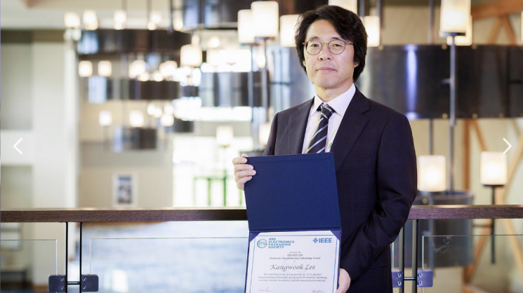 Lee Kang-wook, Vice President in charge of PKG Development at SK Hynix, became the first Korean to receive the "Electronic Manufacturing Technology Award" at the "IEEE Electronics Packaging Society (EPS) Awards 2024."
 [Photo by SK Hynix]
On the 31st, SK Hynix announced that Vice President Lee received the Electronic Manufacturing Technology Award at the 'IEEE EPS Awards 2024' held on the 30th (local time) in Denver, Colorado, USA.
The IEEE EPS Awards is an annual event hosted by EPS under IEEE, the most prestigious organization in the international electrical and electronics engineering field. The Electronic Manufacturing Technology Award is given to individuals who have achieved outstanding accomplishments in the fields of electronics and semiconductor packaging. Since the first recipient in 1996, this is the first time a Korean has received this award.
EPS stated, "Vice President Lee has made significant contributions by leading the development and manufacturing technology advancements of high-bandwidth memory (HBM), an artificial intelligence (AI) memory, through over 20 years of research and development activities in 3D packaging and integrated circuit fields in the global academic and industrial sectors."
Vice President Lee earned his Ph.D. in 2000 from Tohoku University in Japan, specializing in '3D integration technology for implementing integrated microsystems.' After serving as a postdoctoral researcher at Rensselaer Polytechnic Institute in the United States and as a professor at Tohoku University in Japan, he has led the development of packaging technology necessary for HBM products as the head of wafer-level package (WLP) development at SK Hynix since 2018.
In particular, Vice President Lee played a crucial role in SK Hynix securing market leadership in HBM and advancing as a global AI memory leader by successfully introducing the MR-MUF technology, an innovative packaging technology, during the development of the third-generation HBM product, HBM2E, in 2019.
The MR-MUF technology is a process that injects and solidifies a liquid protective material into the space between stacked semiconductor chips to protect the circuits between chips. Compared to the method of laying film-type materials each time a chip is stacked, it is more efficient and effective for heat dissipation.
Vice President Lee said, "I am very pleased that SK Hynix’s outstanding achievements in the HBM field have been officially recognized through this award. As the AI era is fully underway and the role of packaging becomes increasingly important, I will continue to do my best to drive technological innovation."
© The Asia Business Daily(www.asiae.co.kr). All rights reserved.
![Clutching a Stolen Dior Bag, Saying "I Hate Being Poor but Real"... The Grotesque Con of a "Human Knockoff" [Slate]](https://cwcontent.asiae.co.kr/asiaresize/183/2026021902243444107_1771435474.jpg)


